4-3 PLL CIRCUITS
4-3-1 PLL CIRCUIT
A PLL circuit provides stable oscillation of the transmit fre-
quency and receive 1st LO frequency. The PLL output com-
pares the phase of the divided VCO frequency to the refer-
ence frequency. The PLL output frequency is controlled by
the divided ratio (N-data) of a programmable divider.
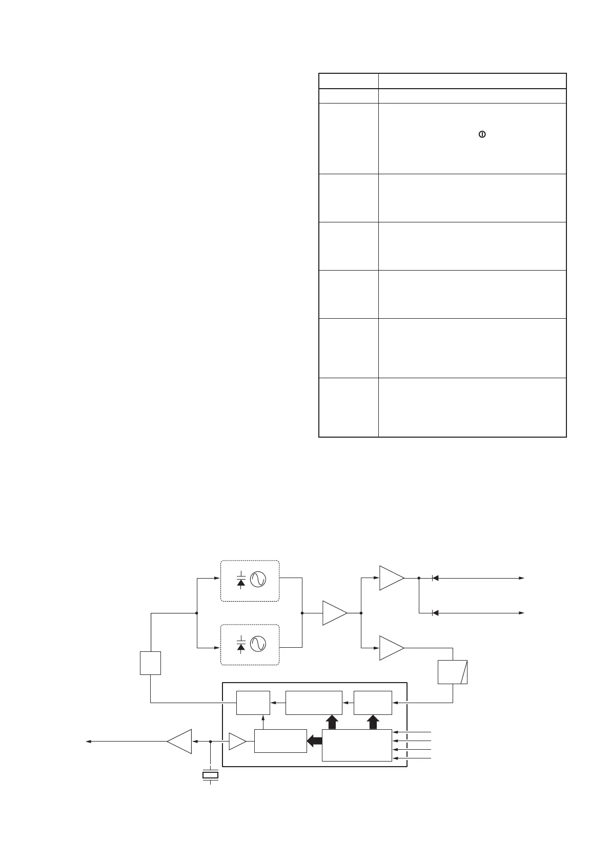
The PLL circuit contains the RX VCO (Q13, D16, D50–D52)
and TX VCO (Q14, D17, D53–D55). The oscillated signal is
amplified at the buffer amplifiers (Q11, Q12) and then ap-
plied to the PLL IC (IC4, pin 17) via the low-pass filter (L32,
C298, C299, C509).
The PLL IC (IC4) contains a prescaler, programmable coun-
ter, programmable divider and phase detector, etc. The ap-
plied signal is divided at the prescaler and programmable
counter section by the N-data ratio from the CPU (IC20). The
reference signal is generated at the reference oscillator (X2)
and is applied to the PLL IC. The PLL IC detects the out-of-
step phase using the reference frequency and outputs it from
pin 13. The output signal is passed thorough the charge
pump (Q50, Q51, Q54, Q55) and loop filter (Q52, Q53), and
is then applied to the VCO circuit as the lock voltage.
If the oscillated signal drifts, its phase changes from that of
the reference frequency, causing a lock voltage change to
compensate for the drift in the oscillated frequency.
4-3-2 VCO CIRCUIT
The VCO circuit contains a separate RX VCO (Q13, D16,
D50–D52) and TX VCO (Q14, D17, D53–D55). The oscil-
lated signal is amplified at the buffer amplifiers (Q10, Q11)
and is then applied to the T/R switch circuit (D14, D15). Then
the receive 1st LO (Rx) signal is applied to the 1st mixer (Q3)
and the transmit (Tx) signal to the YGR amplifier circuit (Q9).
A portion of the signal from the buffer amplifier (Q11) is fed
back to the PLL IC (IC4, pin 17) via the buffer amplifier (Q12)
and low-pass filter (L32, C298, C299, C509) as the compari-
son signal.
Controller
×3
Prescaler
Phase
detector
Loop
filter
Programable
counter
Programable
divider
X2
15.3 MHz
45.9 MHz signal
to the FM IF IC
10
Q13, D16
RX VCO
TX VCO
Buffer
Buffer
Buffer
Q10
Q12
Q11
Q34
20
19
21
22
FSW2
IC4 (PLL IC)
SO
SCK
to transmitter circuit
to 1st mixer circuit
D15
D14
13
17
Q14, D17
LPF
• PLL CIRCUIT
4 - 4
4-4 POWER SUPPLY CIRCUITS
LINE DESCRIPTION
HV The voltage from a DC power supply.
VCC
The same voltage as the HV line which is
controlled by the power switching circuit
(Q23, Q24). When the [ ] switch is pushed,
the CPU outputs the "PWR" control signal to
the power switching circuit to turn the circuit
ON.
CPU5V
Common 5 V converted from the HV line
at the CPU5V regulator circuit (IC10). The
output voltage is applied to the CPU (IC20),
EEPROM
(IC23), etc.
5V
Common 5 V converted from the VCC line at
the 5 V regulator circuit (Q27, Q28). The out-
put voltage is applied to the FM IF IC (IC1),
PLL IC (IC4), etc.
8V
Common 8 V converted from the VCC line
at the 8 V regulator circuit (IC9). The out-
put voltage is applied to the buffer amplifi er
(Q11), AF amplifi er (IC16), etc.
T8V
Transmit 8 V controlled by the T8V regulator
circuit (Q25, Q29, D23) using the "TMUT"
signal from the CPU (IC20, pin 17). The out-
put voltage is applied to the YGR amplifier
(Q9), driver amplifi er (Q10), etc.
R8V
Receive 8 V controlled by the R8V regulator
circuit (Q26, Q30, D24) using the "TXC" sig-
nal from the CPU (IC20, pin 16). The output
voltage is applied to the RF amplifier (Q2),
1st IF amplifi er (Q4), etc.
 Loading...