4 - 3
4-2 TRANSMITTER CIRCUITS
4-2-1 MICROPHONE AMPLIFIER CIRCUIT
(MAIN UNIT)
The microphone amplifier circuit amplifies audio signals
within +6 dB/octave pre-emphasis characteristics from the
microphone to a level needed for the modulation circuit.
The AF signals (MIC) from the microphone (FRONT unit; J1,
pin 6) are applied to the microphone amplifier (FRONT unit;
IC2, pins 3, 4) and then applied to the MAIN unit via J2 (pin 1).
The amplified signals are passed through the D/A converter
(IC6, pins 9, 10) and are then applied to the microphone
amplifier section of the compander IC (IC14, pin 12). The
amplified signals are passed through the compressor, low-
pass filter and high-pass filter sections and output from pin 9
(IC14).
The filtered AF signals are amplified at the buffer amplifier
(Q21) and pre-emphasized with +6dB/octave at the pre-
emphasis circuit (R122, C187), and are then applied to the
IDC amplifier section in IC14 (pin 8).
The amplified AF signals are passed through the limitter
amplifier, low-pass filter, smoothing filter sections after being
passed through the AF mute switch and is then output from
pin 7 (IC14).
The output signals from (IC14) are passed through the PM/
FM switch (IC15, pins 1, 6, 7), splatter filter (IC21, pins 12,
14) and are then applied to the D/A converter (IC6, pins 21,
22). The signals are applied to modulation circuit.
4-2-2 MODULATION CIRCUIT (MAIN UNIT)
The modulation circuit modulates the VCO oscillating signal
(RF signal) using the microphone audio signals.
The AF signals from the D/A converter (IC6, pin 22) change
the reactance of varactor diode (D18) to modulate the oscil-
lated signal at the TX VCO circuit (Q14, D17, D53–D55). The
modulated VCO signal is amplified at the buffer amplifiers
(Q10, Q11) and is then applied to the drive amplifier circuit
via the T/R switch (D14).
The CTCSS/DTCS signals ("CENC0," "CENC1," "CENC2")
from the CPU (IC20, pins 89–91) are combined at resistors
(R267–R269) and are then passed through the low-pass fil-
ter (Q37), D/A converter (IC6, pins 11, 12) and mixer (IC21,
pins 1, 2). The signals are mixed with the AF signals from
the PM/FM switch (IC15, pin 1) and are then applied to D18
in the VCO circuit via the splatter filter (IC21, pins 12, 14).
4-2-3 DRIVE AMPLIFIER CIRCUIT (MAIN UNIT)
The drive amplifier circuit amplifies the VCO oscillating signal
to the level needed at the power amplifier.
The RF signal from the buffer amplifier (Q10) passes through
the T/R switch (D14) and is amplified at the YGR (Q9) and
drive (Q8) amplifiers. The amplified signal is applied to the
power amplifier circuit.
4-2-4 POWER AMPLIFIER CIRCUIT (MAIN UNIT)
The power amplifier circuit amplifies the driver signals to an
output power level.
The RF signal from the drive amplifier (Q8) is applied to the
power module (IC3) to obtain 25 W (for IC-F510/F520, 50
W; for IC-F521) of RF power after pass through the low-pass
filter (L18, C89, C90) and attenuator (D72).
The amplified signal is passed through the low-pass fil-
ter (L15, C387, C388), antenna switching circuit (D2, D3),
low-pass filter (L2, L3, C6–C8) and power detector (D1,
D11), low-pass filter (L1, C1, C2) and is then applied to the
antenna connector (CHASSIS; J1).
Control voltage for the power amplifier (IC3, pin 3) comes
from the APC amplifier (IC2, pin 4) to stabilize the output
power. The transmit mute switch (D32) controls the APC am-
plifier when transmit mute is necessary.
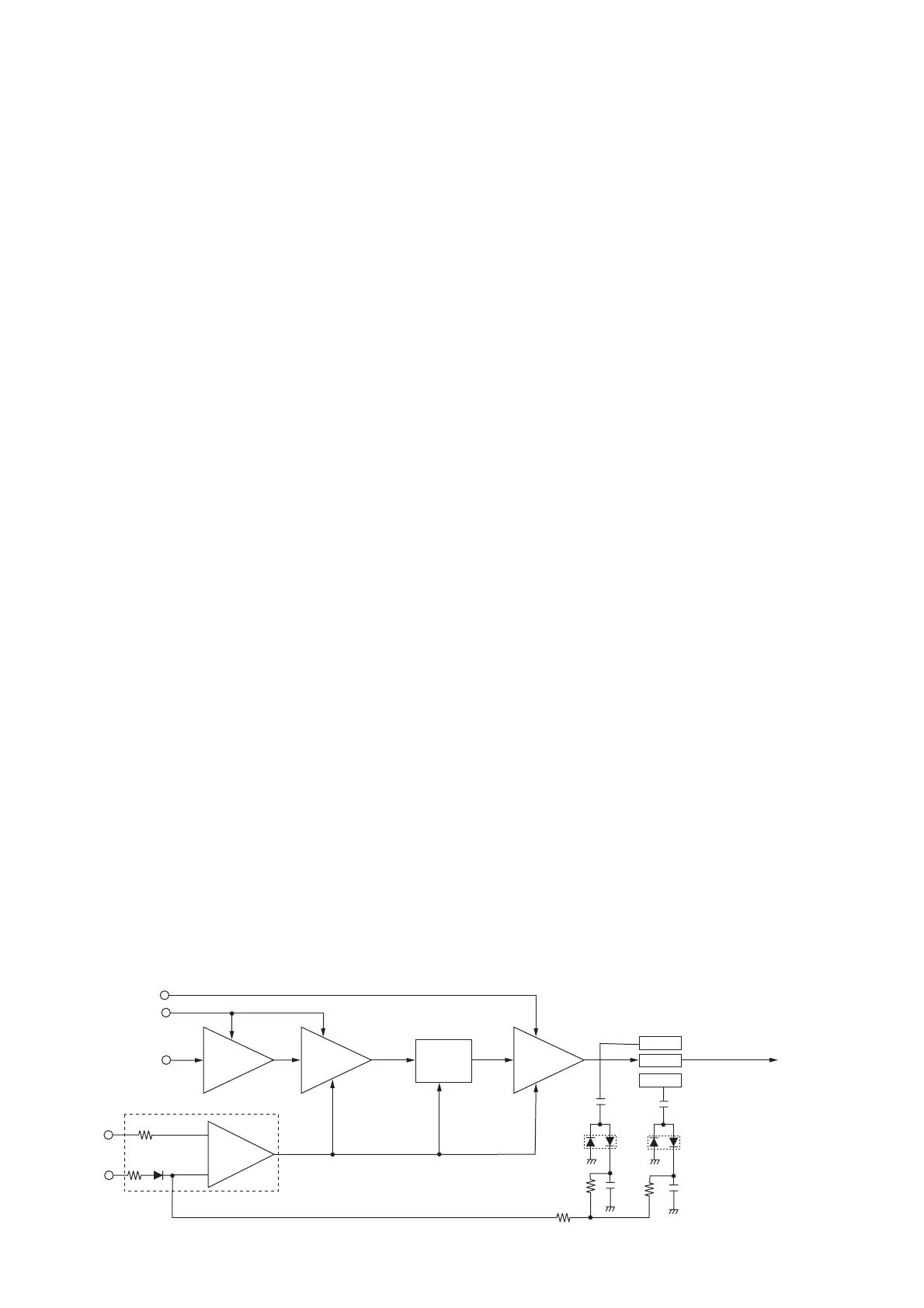
4-2-5 APC CIRCUIT (MAIN UNIT)
The APC circuit protects the power amplifier from a mis-
matched output load and stabilizes the output power.
The power detector circuit (D1, D11) detects forward sig-
nals and reflection signals and converts it into DC voltage.
The detected voltage is at minimum level when the antenna
impedance is matched at 50 Ω, and is increased when it is
mismatched.
The detected voltage is applied to the APC amplifier (IC2,
pin 3), and the power setting “T4” signal from the D/A con-
verter (IC7, pin 4), controlled by the CPU (IC20), is applied to
the another input for reference. When antenna impedance is
mismatched, the detected voltage exceeds the power setting
voltage. Then the output voltage of the APC amplifier (IC2,
pin 4) controls the input voltage of the pre-drive amplifier (Q8),
attenuator (D72), power module (IC3) to reduce the output
power.
POWER
AMP.
ATTE-
NUATOR
APC
AMP.
DRIVE
AMP.
+
–
VCC
to antenna
connector
T4
TMUT
RF signal
from PLL circuit
T8V
APC control circuit
D1
D11
FOR
REV
Q8
D72
Q9
IC2
IC3
YGR
AMP.
• APC CIRCUIT
 Loading...