4 - 3
4-2 TRANSMITTER CIRCUITS
4-2-1 MICROPHONE AMPLIFIER CIRCUIT
(FRONT AND MAIN UNITS)
The microphone amplifier circuit amplifies the audio signals
from microphone within +6 dB/oct pre-emphasis characteris-
tic. The microphone signals are processed in the base band
IC which contains microphone amplifier, compressor, scram-
bler, limiter, splatter filter, etc. in its package.
The audio signals from the microphone (FRONT UNIT;
MC201) are passed through the microphone mute switch
(FRONT UNIT; IC204 pins 1, 2). The switched signals are
amplified at the microphone amplifiers (FRONT UNIT;
IC203, pins 1, 2, 13, 14) to obtain within +6 dB/oct pre-
emphasis characteristics. The amplified signals are applied
to the MAIN UNIT via J1 (pin 2).
The amplified MIC signals from the FRONT UNIT are
applied to the base band IC (IC301, pin 3). The applied
MIC signals are amplified at the amplifier section, and level
adjusted at the volume control section. The level adjusted
MIC signals are applied or bypassed the compressor, pre-
emphasis, TX/RX HPF, scrambler, limiter and splatter sec-
tions in sequence, then applied to another volume controller.
The compressor compresses the MIC signals to provide
high S/N ratio for receive side, and the pre-emphasis obtains
+6 dB/oct audio characteristics. The TX/RX HPF filters out
250 Hz and lower audio signals, the limiter limits its level
and the splatter filters out 3 kHz and higher audio signals.
The filtered MIC signals are level adjusted at another vol-
ume control section and amplified at the amplifier section,
and then output from pin 7 via smoothing section (SMF).
4-2-2 MODULATION CIRCUIT (MAIN UNIT)
The modulation circuit modulates the VCO oscillating signal
with the audio signals from the microphone.
MIC signals from the base band IC (IC301) are passed
through the MIC switch (IC302, pins 4, 5), PM filter (C338,
R327), FM/PM switch (IC302, pins 1, 15), and then applied
to the AF mixer (IC12, pin 2) to be mixed with CTCSS/DTCS
signals.
The mixed MIC signals are output from pin 1 and then
applied to the D/A converter (IC303, pin 4) to be adjusted
its level. The level adjusted AF signals are output from pin 3
and applied to the modulation circuit (D611) to modulate the
VCO oscillating signal by changing the reactance of D611 at
the TX VCO (Q602, D608, D609).
The CTCSS/DTCS signals are generated by the CPU (IC307)
and output from pins 89–91 (“CENC0,” “CENC1,” ”CENC2”).
The CTCSS/DTCS signals are passed through 3 regis-
ters (R374–R376) to change its wave form. The wave form
changed CTCSS/DTCS signals are then passed through the
LPF (IC12, pins 8, 10) and applied to the converter (IC303,
pin 9) to be adjusted its level, and output from pin 10.
The level adjusted CTCSS/DTCS signals are applied to
the AF mixer (IC12, pin 2) to be mixed with MIC signals.
The mixed CTCSS/DTCS signals are output from pin 1 and
applied to the D/A converter (IC303, pin 4) to be adjusted
its level again, then output from pin 3. The CTCSS/DTCS
signals from the D/A converter are applied to the both of
reference frequency oscillator (X1) and modulation circuit
(D611) to modulate the reference frequency signal and VCO
oscillating signal.
The modulated VCO output signal is amplified at the buffer
amplifiers (Q605, Q606, Q609) and is then applied to the
pre-drive amplifier (Q201) via the TX/RX switch (D200).
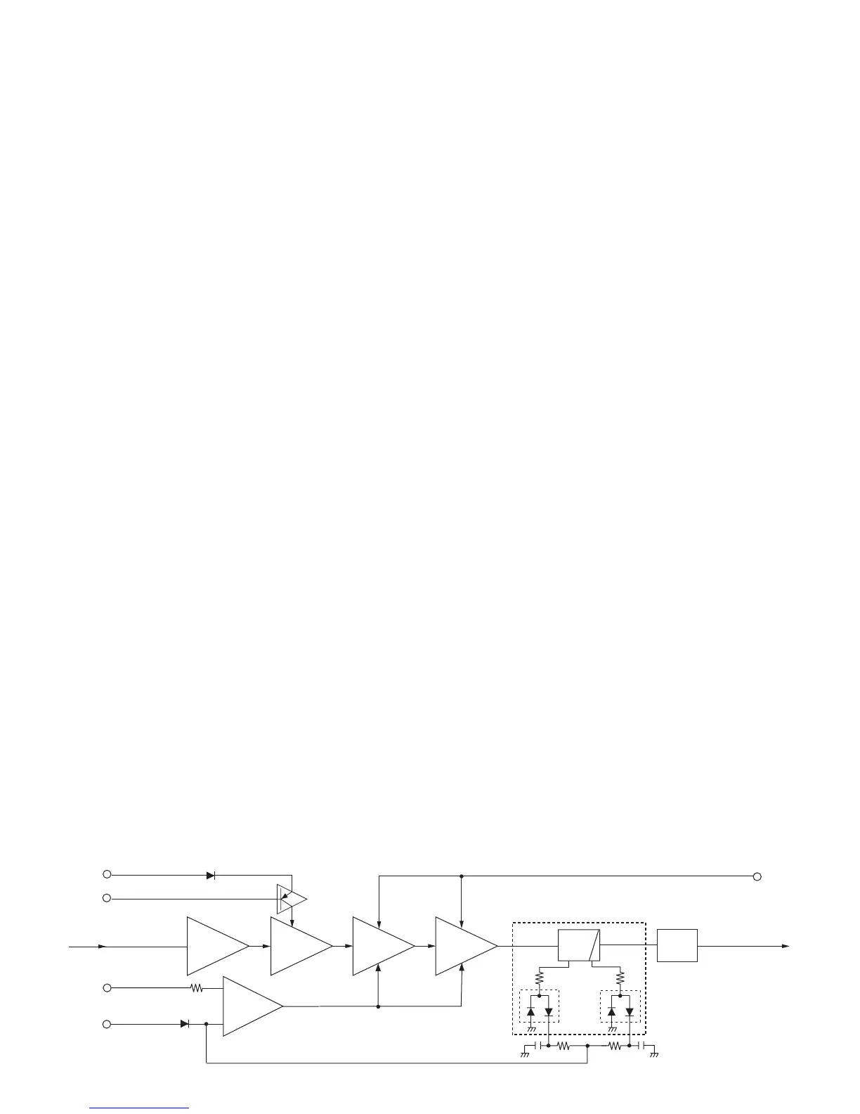
4-2-3 TRANSMIT AMPLIFIERS (MAIN UNIT)
The VCO output signal is amplified to transmit output power
level by the transmit amplifiers .
The buffer-amplified signal from the TX/RX switch (D200)
is applied to the pre-drive (Q201), drive (Q202), and power
(Q203) amplifiers to be amplified to the transmit output power
level.The power amplified transmit signal is passed through
the power detector (D202, D204), antenna switch (D203),
and two-stage LPFs (L522, L523, C565–C569), and then
applied to the antenna connector (CHASSIS UNIT; J1).
4-2-4 APC CIRCUIT (MAIN UNIT)
The APC (Automatic Power Control) circuit stabilizes trans-
mit output power and controls transmit output power High or
Low.
The power detector circuits (D202, D204) detect the transmit
output signal level and converts it into DC voltage.
The detected voltage is applied to the APC amplifier (IC200,
pin 3). The “T2” signal from the D/A converter (IC310, pin
2), controlled by the CPU (IC307), is applied to the another
input (pin 1) for reference, and the "T2" signal also controls
transmit output power (4 W, 2 W or 1 W).
The output voltage from the APC amplifier controls the bias
of the drive amplifier (Q202) and power amplifier (Q203) to
control the output power by comparing the detected voltage
and the reference voltage. Thus the APC circuit maintains a
constant transmit output power.
Power
amp.
APC
amp.
Drive
amp.
+
–
VCC
• APC CIRCUIT
to the anntena
T2
TMUT
TMUT
from TX/RX switch
(D200, D501)
T5V
Q202
Buffer
amp.
Pre-drive
amp.
Q201Q200
IC200
Q203
LPF
ANT
SW
Q204
D205
D202
Power detector
D204
D203
 Loading...