4 - 5
A portion of the AF signals from the FM IF IC (RF unit; IC2,
pin 9) are applied to the active filter section (IC2, pin 8). The
active filter section amplifies and filters noise components.
The filtered signals are applied to the noise detector section
and output from pin 13 as the “SDET” signal.
The “SDET” signal from IC2 (pin 13) is applied to the CPU
(LOGIC unit; IC11, pin 12) directly. The CPU analyzes the
noise condition and outputs the “AMUTE” signal to the AF
mute switch (Q37).
Even when the squelch is closed, the AF mute switch (Q37)
opens at the moment of emitting beep tones.
• TONE SQUELCH
The tone squelch circuit detects AF signals and opens the
squelch only when receiving a signal containing a matching
subaudible tone (CTCSS). When tone squelch is in use, and
a signal with a mismatched or no subaudible tone is
received, the tone squelch circuit mutes the AF signals even
when noise squelch is open.
A portion of the AF signals from the FM IF IC (RF unit; IC2,
pin 9) passes through the low-pass filter (LOGIC unit; IC9)
via the “FMAF” signal to remove AF (voice) signals and
passes through the tone filter (LOGIC unit; IC9, Q8). The fil-
tered signal is applied to the CTCSS decoder inside CPU
(LOGIC unit; IC11, pin 8) via the “RTONE” line to control the
AF mute switch.
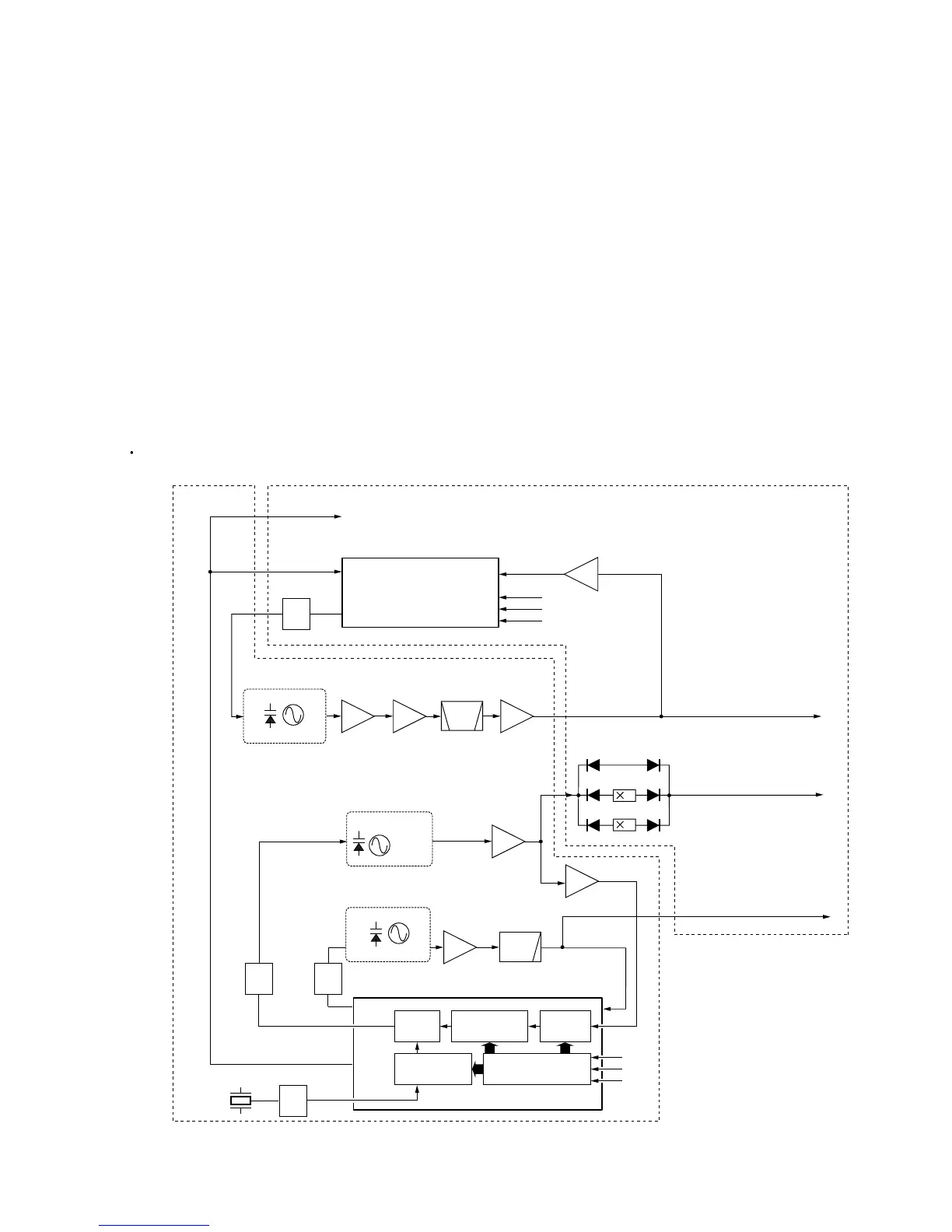
4-2 PLL CIRCUITS
4-2-1 PLL CIRCUIT (VCO UNIT)
A PLL circuit provides stable oscillation of the receive
1st/2nd LO frequencies. The PLL circuit compares the
phase of the divided VCO frequency to the reference fre-
quency. The PLL output frequency is controlled by the divid-
ed ratio (N-data) of a programmable divider.
PLL CIRCUIT
Shift register
Prescaler
Phase
detector
Loop
filter
Loop
filter
Programmable
counter
Programmable
divider
X1
12.8 MHz
Buff.
Q25
D63D64
D65D67
D66D68
IC4
3
4
5
PSTB
IC3 (PLL IC)
PCK
PDA
16
13
17
19
1st VCO
Q22,
Q23,
D62
Q31,
Q32
8
Loop
filter
Q870,
Q871
Buff.
Q853
D41
2
"2nd LO" signal to the 2nd mixer
circuit (IC10, pin 3)
"1st LO" signal to the 1st mixer
circuit (IC1, pin 3)
"CONLO" signal to the converter
mixer circuit (IC13, pin 3)
2nd VCO
Q34, D202
Converter VCO
Q861, D913
Amp.
Amp.
Buff.
Q862
RF
Q863
LPF
RF
Q864
Q874
2
2
VXO
IC15
(Converter PLL IC)
RF UNIT
VCO UNIT
3
4
5
PCK
PDA
PSTB
1
6
"REF" signal to the FM IF IC
(IC2, pin 2)
10
BPF
 Loading...