SECTION 4 CIRCUIT DESCRIPTION
4 - 1
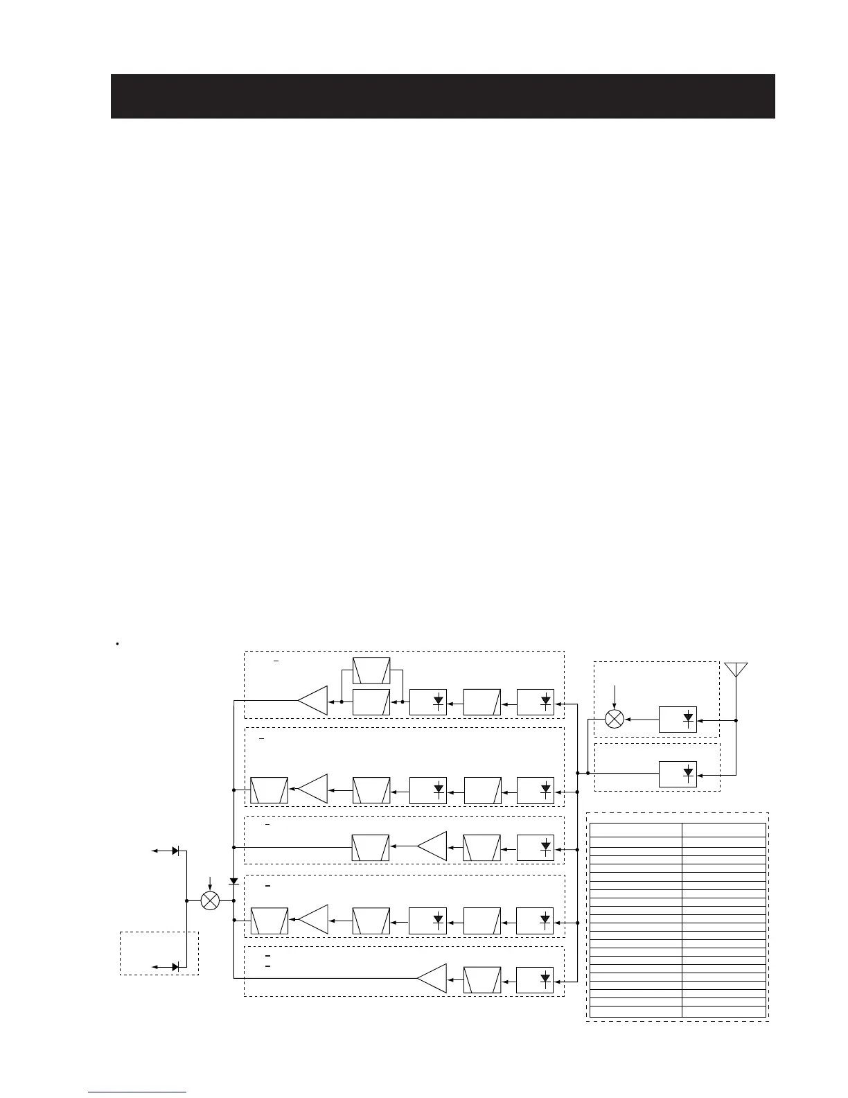
4-1 RECEIVER CIRCUITS
4-1-1 RF SWITCHING CIRCUIT (RF UNIT)
(1) Below 1150 MHz
The RF signals from the antenna connector pass through
the band switching diode (D2) and an attenuator (D12, D13).
The signals are then applied to the RF circuit which sup-
press out-of-band signals via the band switching diode
(D911).
(2) Above 1150 MHz
The RF signals from the antenna connector pass through
the limitter (D1), band switching diode (D909) and high-pass
filter (C932–C936, C963, C964, L911, L912, L914). The fil-
tered signals are applied to the AF amplifier (IC14, pin 1),
and are then applied to the convertor circuit (IC13, pin 1).
Above 1150 MHz RF signals are mixed with “CONLO” signal
from CONV VCO circuit for convertion into below 1150 MHz
RF signals at the converter circuit (IC13). The converted sig-
nals are output from IC13 (pin 6), and are then applied to the
RF circuit which suppress out-of-band signals.
4-1-2 RF CIRCUIT (RF AND RF-B UNITS)
The RF circuit amplifies the received signals within the
range of frequency coverage and filters out-of-band signals.
(1) 0.495 MHz–29.995 MHz
RF signals (0.495 MHz–29.995 MHz) from the RF switching
circuit pass through a low-pass filter (C321–C325, L81,
L82). The filtered signals are amplified at an RF amplifier
(Q3) passing through each low-pass, bandpass, high-pass
filter depending on the receiving frequency. The amplified
signals are then applied to the 1st mixer circuit (IC1) via the
band switching diode (D10).
The signals below 1.9 MHz pass through a low-pass filter
(C344–C347, L89, L90) between the band switching diode
(D4, D7), and are then applied to the RF amplifier circuit
(Q3).
The 1.9 MHz–14.995 MHz signals pass through the band
switching diode (D5) and bandpass filter (C332–C341,
L85–L88), and are then applied to the RF amplifier circuit
(Q3) via the band switching diode (D8).
The 15 MHz–29.995 MHz signals pass through the band
switching diode (D6) and high-pass filter (C326–C330, L83,
L84) and are then applied to the RF amplifier circuit (Q3) via
the band switching diode (D9).
(2) 30 MHz–224.995 MHz (RF-B UNIT)
RF signals (30 MHz–64.995 MHz, 65 MHz–107.995 MHz,
108 MHz–173.995 MHz, 174 MHz–224.995 MHz) from the
RF switching diode (RF unit; D11) are passed through the
low-pass filter (RF unit; C12–C17, L57–L59). The filtered
signals pass through the each bandpass filters and RF
amplifier depending on the receiving frequency. The signals
are then applied to the 1st mixer circuit (RF unit; IC1).
The 30 MHz–64.995 MHz signals pass through the band
switching diode (D403) and bandpass filter (D401), and are
then amplified at the RF amplifier (Q401). The amplified sig-
nals pass through the bandpass filter (D402) and band
switching diode (D404).
 Loading...