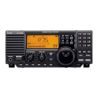
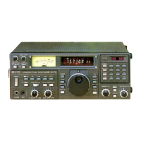
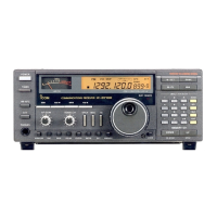
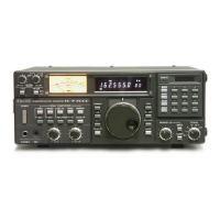
3 - 5
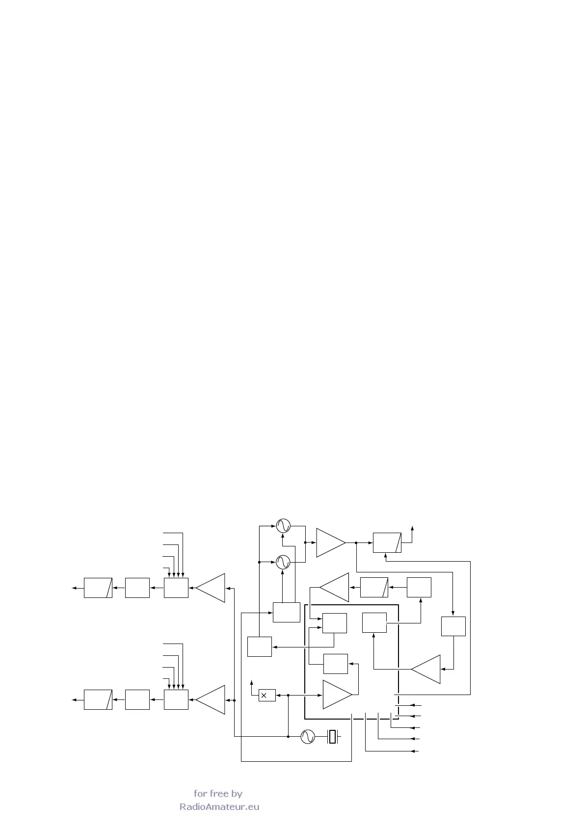
The oscillated signal at the VCO1 and VCO2 circuit is ampli-
fied at the LO-amplifier (PLL unit; Q91), and passes through
the low-pass filter (PLL unit; Q92, D91, D92, L91, L93,
C96–C100, C102, C103) to supperss high harmonic compo-
nents. The low-pass filter controlls the cut-off frequency of
less than 29.999 MHz and more than 30.000 MHz by switch-
ing C102 and C103 “ON” and “OFF” respectively.
The filtered signal is applied to the LO-amplifier (MAIN unit;
Q411), and is then applied to the 1st mixer circuit (MAIN unit;
Q441, Q442) via the low-pass filter (MAIN unit; L421, L422,
C422–C425).
The reference frequency from the LO-amplifier (PLL unit;
Q91) is also divided by 4 at IC22, and is amplified at the
IC23. The signal is applied to the DDS-IC (PLL unit; IC21, pin
88) for the clock signal.
3-2-4 2ND LO CIRCUIT (PLL AND MAIN UNIT)
The 30 MHz reference frequency from the Q1 and X1 on the
PLL unit is multiplied by 2 at Q2 on the PLL unit. The 60 MHz
2nd LO signal is obtained at the L4 and L5 on the MAIN unit,
and is then applied to the 2nd mixer circuit (MAIN unit; D491)
via the 3dB attenuator (MAIN UNIT; R491–R493).
3-2-5 3RD LO CIRCUIT (PLL AND MAIN UNIT)
The 30 MHz reference frequency is oscillated at the Q1 and
X1 on the PLL unit, and is then amplified at the Q151 on the
PLL unit. The amplified signal is applied to the 10 bits DDS-
IC (PLL unit; IC151, pin 7) for the clock signal to produce the
9.4665 MHz 3rd LO signal. The 3rd LO signal is applied to
the D/A converter circuit, and passes through the low-pass
filter (PLL unit; L151, L152, C152–C157) to suppress spuri-
ous components. The filtered 9.4665 MHz 3rd LO signal is
applied to the 3rd mixer circuit (MAIN unit; IC811, pin 10)
3-2-6 BFO CIRCUIT (PLL AND MAIN UNIT)
The 30 MHz reference frequency is amplified at the Q201 on
the PLL unit, and is applied to the 10 bits DDS-IC (PLL unit;
IC201, pin 7) for the clock signal to produce the 455 kHz BFO
signal. The BFO signal is applied to the D/A converter circuit,
and passes through the low-pass filter (PLL unit, L201, L202,
C202–C207) to suppress spurious components. The filtered
455 kHz BFO signal is applied to the BFO mixer circuit (MAIN
unit; IC1101, pin 10).
3-2-7 VCO CIRCUIT
The VCO circuit consists of the VCO1 circuit (PLL unit; Q71,
Q72, D71) and VCO2 circuit (PLL unit; Q81, Q82, D81).
The VCO1 controls less than displayed frequency of 29.999
MHz to use the PLL lock voltage from the DDS-IC.
The VCO2 controls more than displayed frequency of 30.000
MHz to use the PLL lock voltage from the DDS-IC.
3-3 LOGIC CIRCUITS
The LOGIC circuit consists of the CPU, the reset circuit,
backup battery circuit, and so on.
3-3-1 CPU (LOGIC UNIT)
The CPU (IC101) contains 8-bit one chip CPU. The CPU
controls the operating frequency, mode, function, display,
panel switches, panel volumes.
The panel switches are connected the CPU input port to the
function of the panel switch or are connected some functions
of panel switches to the A/D converter input port in the CPU.
The CI-V signal which is used for communicate to the per-
sonal computer is controlled by the level control circuit
(IC401A, IC401B, Q401 and so on).
 Loading...