Intel
®
Pentium
®
III Processor with 512KB L2 Cache Dual Processor Platform Design Guide 4-3
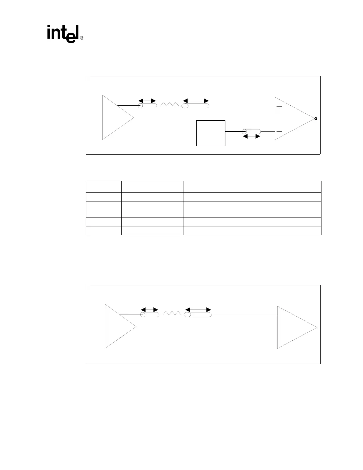
Figure 4-3 shows the topology that should be used for the chipset clock traces. Please note that L0 and
L1 refer to trace lengths between the illustrated components. Ta ble 4-2 contains the recommended
lengths and component values for this topology.
Figure 4-2. Single Ended Clocking Topology - CPU
Table 4-1. Component Values for SE Clocking Topology - CPU
Reference Value Notes
L0 0.25 to 0.5 inches All L0s should be matched
L1
Chipset L1 + 1” +/- 0.125
Chipset L1 + 0.5” +/- 0.125
Use this processor L1 length if the chipset L1 is 5”-7”
Use this processor L1 length if the chipset L1 is 7”-12”
L2 0.0 to 1.0 inches L2 should be as short as possible.
Rs 22 to 33 Ω 1% Tolerance
Figure 4-3. Single Ended Clocking Topology - Chipset
BCLK
CLKREF
Clock Driver
Processor
Rs
Zo = 60 ohm
L2
Zo = 60 ohm
L0
L1
W37
Y33
CLKREF
Filter
CLK
Clock Driver
Chipset
Rs
Zo = 60 ohm
Zo = 60 ohm
L0
L1

 Loading...