Intel
®
Pentium
®
III Processor with 512KB L2 Cache Dual Processor Platform Design Guide 4-5
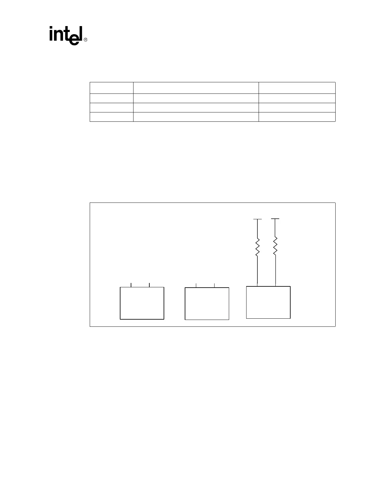
4.2.2 Single-Ended Clocking BSEL[1:0] Implementation
In an Intel
®
Pentium
®
III Processor with 512KB L2 Cache platform that is using single-ended (SE)
clocking or a clock source that does not support the VTT_PWRGD protocol, the normal BSEL frequency
selection process will not work. Since the clock generator is not compatible with dynamic BSEL
assertions, all BSEL[1:0] signals should not be connected together. Instead, the BSEL pins on the clock
generator should be pulled-up to 3.3 V through a 1 KΩ, 5% resistor. This strapping will force the clock
generator into 133 MHz clocking mode and will only support 133 MHz capable processors.
4.3 Differential Host Bus Clocking Routing
Intel
®
Pentium
®
III Processor with 512KB L2 Cache dual-processor platforms support differential host
bus clock drivers. When operating in differential clocking mode, the BCLK and BCLK#/CLKREF form a
differential pair of clock inputs. The differential pair of traces should be routed with special care and using
standard differential signalling techniques. The following sections contain the recommended topology
and routing for differential clocking for these platforms.
Table 4-3. CLKREF Component Values
Reference Value Notes
R1 150 Ω 1% Tolerance
R2 150 Ω 1% Tolerance
C1 4.7 µF
Figure 4-5. Single Ended Clock BSEL Circuit
BSEL0
Processor 0
BSEL1
1KΩ
5%
1KΩ
5%
3.3V
3.3V
BSEL0
Clock Driver
BSEL1
BSEL0
Processor 1
BSEL1
NC NCNCNC

 Loading...