4-8 Intel
®
Pentium
®
III Processor with 512KB L2 Cache Dual Processor Platform Design Guide
For a single-ended clock driver design, the topology illustrated in Figure 4-3 should be used. In this case,
the “chipset” in the illustration is actually the debug port pin. The trace length L0 and the Rs value are the
same as recommendations for the chipset in Table 4-2. However, the length of the trace segment L1
should be chosen so that it complies with the requirements described in the previous paragraph. This
means that the L1 for the debug port is at least as long as the L1 for the processor clock traces.
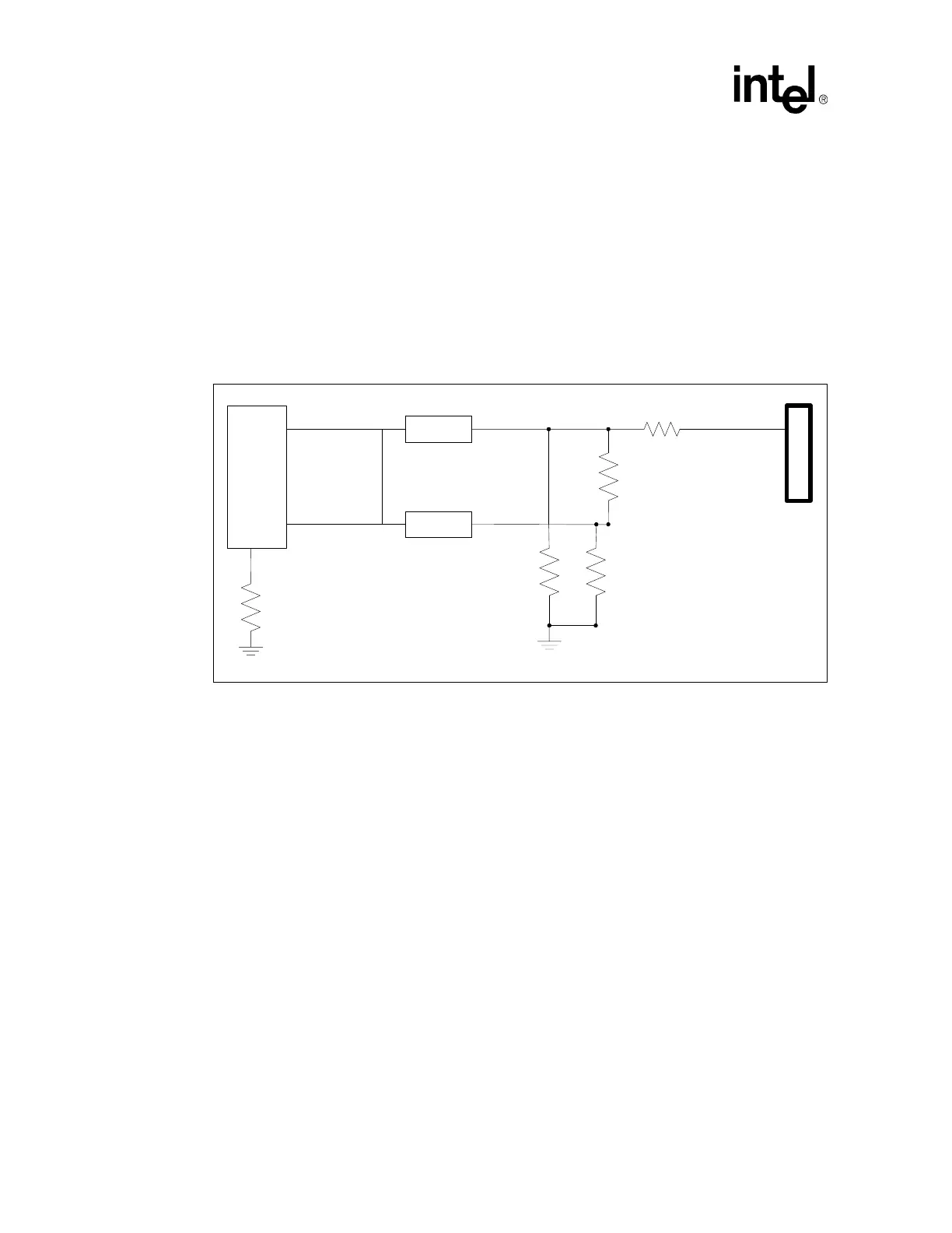
The circuit recommendations for a differential clock driver design are shown in Figure 4-8.Thelength,
L0, should be chosen to complies with the flight time requirements mentioned in this section. Please note
that these requirements will make the length L0 longer than the processor clock trace’s L0 lengths. The
terminating resistors should be placed as close the ITP socket as possible.
4.5 Clock Driver Decoupling and Power Delivery
The decoupling and power delivery requirements of the system clock driver are dependent on the clock
driver and chipset used in the system implementation. Because of this, no specific information can be
provided in this document. However, since proper decoupling and noise-free power delivery are critical to
the clock driver’s operation, Intel encourages system implementors to carefully follow the chipset and
clock driver vendor’s recommendations in these areas. An incorrect implementation of these circuits can
easily cripple a clock driver’s ability to produce reliable clock signals and lead to system instability.
Please refer to the appropriate clock driver and chipset vendor information for more details.
Figure 4-8. Debug Port Differential Host Clock Implementation
Differential
Clock
Driver
L0
L0
33.2 ohms 1%
475 ohms 1%
221 ohms 1%
63.4 ohms 1% 63.4 ohms 1%
BCLK
BCLK#
I
T
P

 Loading...