Intel
®
Pentium
®
III Processor with 512KB L2 Cache Dual Processor Platform Design Guide 4-7
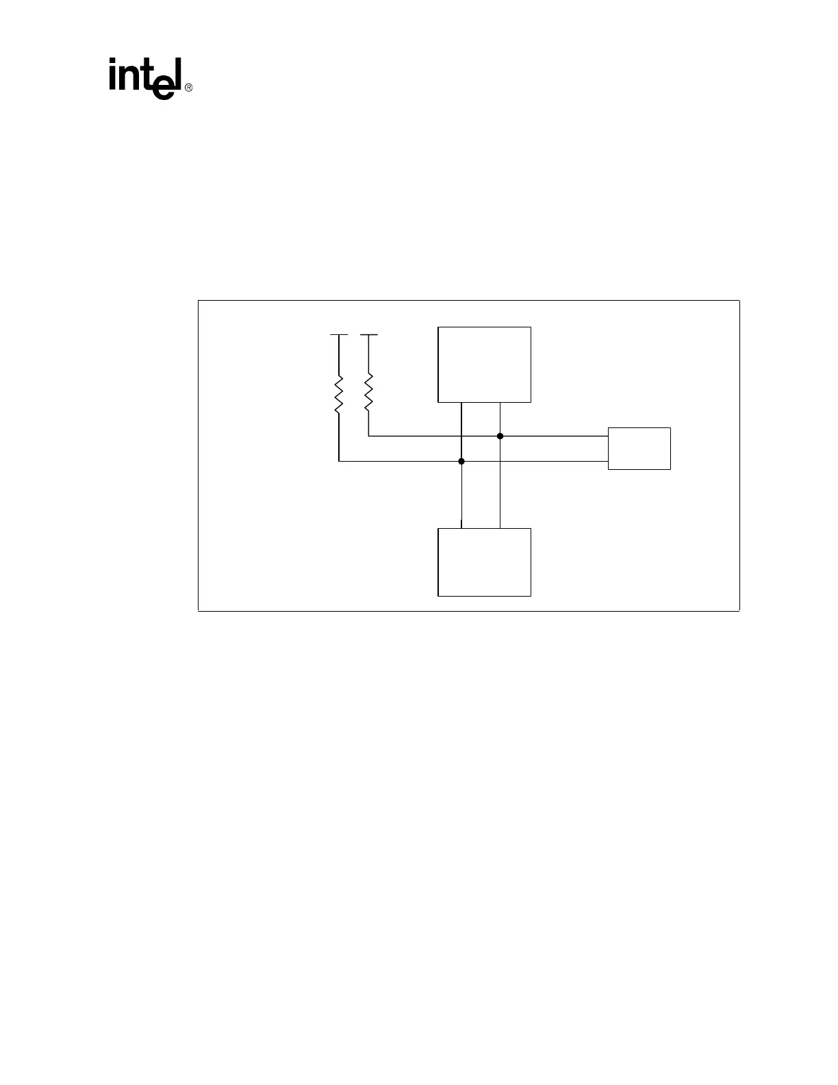
4.3.2 Differential Clocking BSEL[1:0] Implementation
The System Bus Frequency Select Signals (BSEL [1:0]) are used to select the system bus frequency for
the host bus agents. The frequency selection is determined by the processor(s) and driven out to the
host bus clock generator. All system bus agents must operate at the same 133MHz frequency. The BSEL
pins for the processor are open drain signals and rely on a 3.3V pull-up resistor to set the signal to a logic
high level. Figure 4-7 shows the recommended implementation for a differentially clocked system.
4.4 Debug Port Host Clock Connection
In order to recover full front side bus speed BPM[5:0]# and RESET# data with the ITP, the Debug Port
should be placed as close as is physically reasonable to the system bus and no further than 1.5 ns flight
time (as measured by trace length of the BPM[5:0]# and RESET# signals) from the nearest front side
bus agent. System designers should record the flight time of the BPM[5:0]# and RESET# signals from
the nearest front side bus agent to the Debug Port. This value will be important during the routing of
several other Debug Port signals.
Assuming BCLK (and BCLK# in differential clocked systems) signals are routed from the system clock
buffer to each of the synchronous clock agents with a matched length, the copy of this signals from the
system clock buffer to the ITP Debug Port must have a flight time equal to the matched length of the
other synchronous clock agents plus the flight time of the BPM[5:0]# signals from the nearest bus agent
to the Debug Port noted above. This will ensure that the same BCLK to BPM[5:0]# phase relationship
seen at the closest system bus agent will be present at the Debug Port pins. Clock trace lengths may be
adjusted to center the recovery of BPM[5:0]# and RESET# at the Debug Port within the ITP receiver
setupanholdwindow.
Figure 4-7. Differential Clock BSEL Circuit
Processor 0
BSEL0
BSEL1
Clock
Driver
1K ohm
5%
1K ohm
5%
3.3V 3.3V
Processor 1
BSEL0
BSEL1

 Loading...