Troubleshooting
2-75
2.11.19 Absolute value circuit, X10 gain tests
Test 405.1 — Large positive DAC V for X10 gain comparison
Type
Circuit Exercise
Fault message None
Description DAC U433 and op amp pair U430 are set up to generate +0.51 VDC at PRECOMP+ and tied to
ACF through R491and U412. ACF is tied to pin 7 of multiplexer U414. The output of the mul-
tiplexer is tied to the A/D through buffer U403, ACV/A input to U222, and A/D buffer gain is
X1. The value of the DAC voltage is measured and stored. This value will also be applied to the
FWR that will be set for X10 gain in test 405.2. In this manner, the applied value to the X10
FWR and the output value can be compared to check for FWR accuracy.
Components Analog Board; 2002-100
Bit patterns
Test 405.2 — Absolute value X10 gain (non-inverting)
Type
Pass/Fail
Fault message Absolute value gain = 10
Description DAC U433 and op amp pair U430 are set up to generate +0.51 VDC at PRECOMP+ and tied to
ACF through R491 and U412. ACF is tied to AMP IN through U428, Q422, and ACV buffer.
AMP IN is tied to the inverting and non-inverting paths of the FWR. NETOUT from U417 in
the non-inverting path is monitored by the ZERO CROSSING amp for either polarity of input
signal and generates the COMP- signal that is tied to comparator U408. The comparator selects
the path that the AMP IN signal will follow through the FWR with switches in U410. Plus AMP
IN path with FWR X10 is through R452, Q413, Q411, U417, R453, U410, Q404, and U419 to
pin 12 of multiplexer U414. The output of the multiplexer is tied to the A/D through buffer U403,
ACV/A input to U222, and the A/D buffer in X1 gain configuration.
Drawing reference Analog Board; 2002-100
Components U403, U408, U412, U414, U417, U419, U430, U433, and associated components.
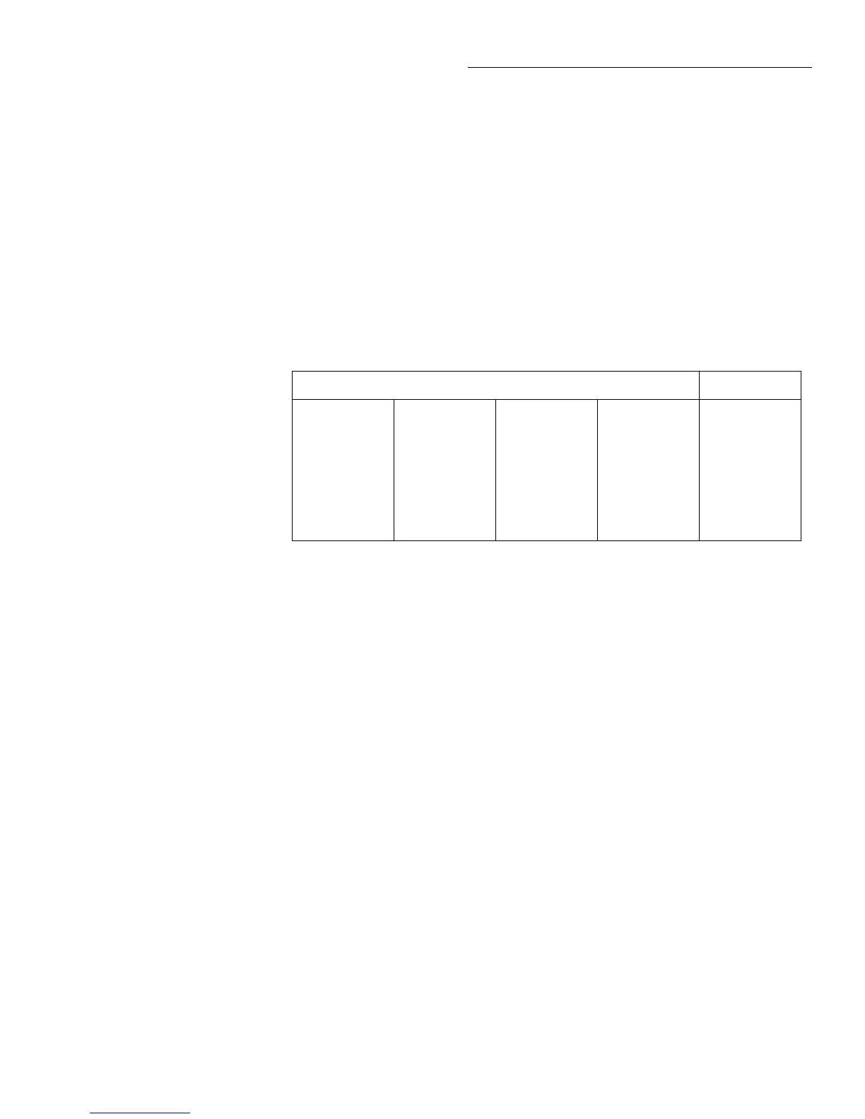
Bit pattern* Register
—U400—
01011011
—U811—
00001101
—U224—
00010111
—U432—
10001101
—U810—
00000011
—U206—
01110000
—U203—
10001110
—U411—
11011111
—U809—
11100111
—U207—
11001111
—U221—
11101001
—U406—
01001111
AD_STB
MUX_STB
R1_STB
R2_STB
*Bits associated with register IC terminals as follows:
QQQQQQQQ
87654321 87654321 87654321 87654321
IC pins: Q8=11, Q7=12, Q6=13, Q5=14, Q4=7, Q3=6, Q2=5, Q1=4.

 Loading...