A920: Charger
Description
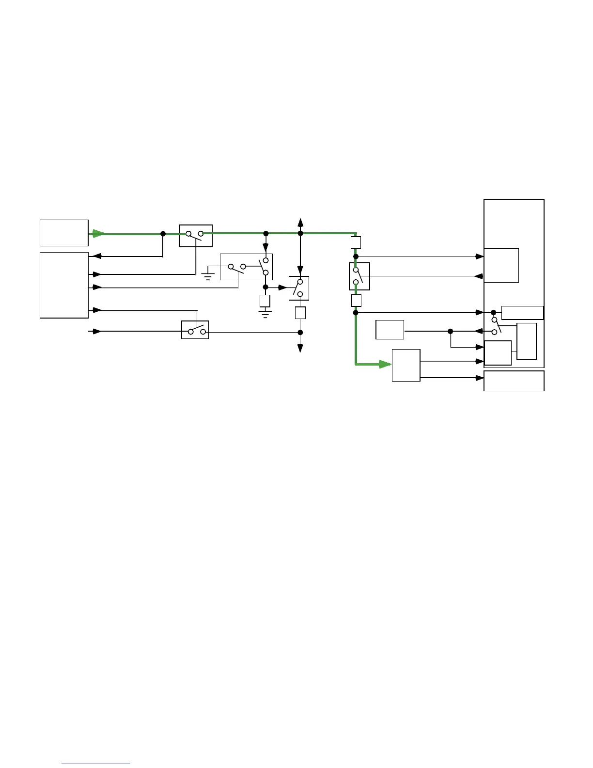
The majority of the charging circuit is integrated in PCAP. This includes a digital to analog converter, analog to digital converter, battery feedback switch, thermistor
switch/pullup, and current control sense. External FETs (Q3966 and Q3954) are provided to enable/disable EXT_B+ and BATTERY supply paths to radio circuitry
(B+). An external sense resistor (R3961) and a charging FET (Q3960) are provided to control charging current between EXT_B+ and BATTERY.
Due to pin count constraints on the CE bus, the Charger Identification input signal and Battery Feedback output signal share the same accessory connector pin. Software
will first detect the Charger ID Voltage (AD6) before enabling the Battery Feedback Voltage via the Battery Feedback Switch in PCAP. The Battery Feedback switch
must not be enabled at any time for an accessory that is not a valid Fast Charger.
Battery Feedback Voltage provides a reference voltage to the external power supply during charging. The battery feedback switch is needed to remove the battery feed-
back voltage from the feedback loop of the AC/DC Adapter or VPA when charging is complete or after a fault has occurred. This switch will be enabled before the char-
ger DAC is programmed when charging is to begin. Battery feedback will turn on before the charger is enabled. The charger will be turned off before battery feedback is
disabled.
A thermistor in the battery package is used to determine cell temperature of the battery pack before charging begins. The battery EPROM (BATT_IO) will contain
limit parameters that determine the minimum and maximum temperatures at which charging can occur.
PCAP has an integrated over-voltage detection circuit that provides protection against damage caused by external charger voltages exceeding 7.0Vdc. If an over-voltage
condition occurs, the EXT_B+ FET (Q3963) will be disabled. This will prevent high voltage (>7Vdc) from being applied to radio circuitry (B+).
Mid-rate charging is supported if a valid mid-rate charger and valid battery are detected. A mid-rate charger will source up to 400mA of current to the radio circuitry and
charging circuitry during idle mode. The mid-rate charger will supply 5.9Vdc (up to 400mA) to the phone, regardless of the BATT_FDBK voltage. If the phone is
in transmit mode, mid-rate current will be supplied to the battery and radio circuitry via the charging path only (EXT_B+ FET (Q3966) will be disabled via the
MIDRATE_1 line). Dead battery TX operation or ‘No Battery’ operation is not supported with a mid-rate charger.
Motorola Confidential Proprietary
4-32
RAW_EXT_B+
EXT_B+
B+
ISENSE
CHRGC
BATT+
MAIN_FET
BATT+
Q3966
Q3967
R5480
CR3961
R3961
Q3960
CR3960
Q3964
Q3963
OV_GATE
OV_SENSE
PCAP
U3000
MIDRATE_1
PCAP
U3000
CE
Conn
Charger
BATT_FDBK
AD6
BATT_THERM
CE
Conn
SPI
MUX
BattSense
BATT_IO
POG
Batt
Conn
 Loading...