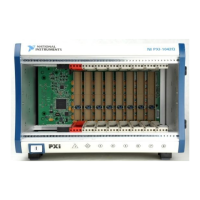
Chapter 2 Installation and Configuration
NI PXI-1042 Series User Manual 2-10 ni.com
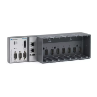
PXI_CLK10 Rear Connectors
There are two BNC connectors on the rear of the PXI-1042 Series chassis
for PXI_CLK10. The connectors are labeled IN and OUT. You can use
them for supplying the backplane with PXI_CLK10 or routing the
backplane’s PXI_CLK10 to another chassis.
10 MHz REF IN
You can use the 10 MHz REF IN connector to supply an external 10 MHz
clock to the backplane. The external clock signal is buffered and provided
to each peripheral slot’s PXI_CLK10 pin with a maximum slot-to-slot
skew of 250 ps. When the backplane detects a 10 MHz signal on the
10 MHz REF IN connector, it automatically overrides the 10 MHz clock
provided by the backplane and uses the externally provided clock. If the
backplane detects a 10 MHz clock on the PXI_CLK10_IN pin of Slot 2 and
a 10 MHz clock on the external 10 MHz REF IN connector, the backplane
automatically selects the signal from Slot 2 and provides that signal to each
peripheral slot.
The input impedance of the 10 MHz REF IN connector on the rear of the
chassis is 50 Ω ±5Ω. The backplane accepts a 10 MHz clock signal
between 200 mV
pp
and 5 V
pp
and rejects any DC component of the
PXI_CLK10 IN signal. The input signal may be a 10 MHz square wave
or sine wave.
10 MHz REF OUT
The 10 MHz REF OUT connector provides a buffered non-TTL version
of the PXI_CLK10 TTL signal supplied to the peripheral slots on the
backplane. You can use this signal to synchronize multiple PXI chassis
to the same PXI_CLK10 signal.
The output impedance of this connector is 50 Ω ±5Ω. The output signal is
a 1 V
pp
±20% non-TTL square wave.
 Loading...