Pin No. Symbol I/O
Descriptions
3AMUT O
Audio muting output pin.
4VB O
Output B pin to control video signal.
5VA O
Output A pin to control video signal.
6 EVDD
Power supply pin. Connect to +5V.
7 EVSS
Ground pin.
8GSW O
Gain control signal output pin for subwoofer.
9GFS O
Gain control output signal pin to front, surround, and center channels.
10 ~CODECPD O
Power down output pin to Codec IC.
11 INTREQ I/O
Interrupter and abort signal input/output pin of DSP IC.
12 DSPDI I
Serial data input pin from DIR and DSP ICs.
13 DSPDO O
Serial data output pin from DIR and DSP ICs.
14 DSPSCK O
Serial clock output pin to DIR and DSP ICs.
15 DSPCS O
Chip select output pin to DSP IC.
16 CSROM/~SRAM O
Change-over pin of RAM and ROM, ROM at H.
17 A15 O
ROM address 15
19 A16 O
ROM address 16
20 A17 O
ROM address 17
21 ~DSPRST O
Reset signal output pin to DSP IC.
22 ERF I
Error flag input pin.
23 AUTO O
Auto detection input pin of DIR IC.
24 DIRCS O
Chip select output pin to DIR IC.
25 ~DIRPD O
Power down signal output pin to DIR IC.
31 ~RESET I
System reset input terminal.
32 XT1
Oscillator connection pin of sub system. Not used.
33 XT2
Not used.
35 X2
Ceramic oscillator connection pins.
36 X1
Connect the 20MHz ceramic oscillator between X1 and X2 pins.
37 VSS
Power supply pin. Connect to ground pin.
38 VDD
Power supply pin. Connect to +5V.
39 CLKOUT
Not used.
41 SPB O
Speaker relay B control signal output pin.
42 SEC1H O
Amplifier gain control output pin.
43 SPCS O
Speaker relay control output pin of center and surround channels.
44 SPA O
Speaker relay A control signal output pin.
45 POWER O
Power relay control output pin.
46 PROTECT I
Protection circuit detection input pin.
47 UPLED O
Up direction LED control output pin of SSC.
48 DNLED O
Down direction LED control output pin of SSC.
49 LEED O
Left direction LED control output pin of SSC.
Pin No. Symbol I/O Descriptions
50 RLED O Right direction LED control output pin of SSC.
51 ~SBMRST O Reset signal output pin to sub microprocessor.
52 SBMCLK O Clock signal output pin to transmit to the sub microprocessor.
53 SBMDO O Data signal output pin to transmit to the sub microprocessor.
54 SBMDI I Data signal input pin to transmit from the sub microprocessor.
55 BVDD Power supply pin. Connect to +5V.
56 BVSS Ground pin.
57 SBMREDY I Read signal input pin to transmit from the sub microprocessor.
58 HD I Detection pin when insert the headphones.
59 Z2LED O Zone 2 LED control output pin.
61 HPMUT O Muting output pin to the headphone circuit.
64 TMUT O Muting output pin to the tuner block.
66 FDA O Data signal output pin to Selector, Configuration, Multi channel, and Multi source control ICs.
67 FCL O Clock signal output pin to Selector, Configuration, Multi channel, and Multi source control ICs.
68 FSTB O Strobe signal output pin to Selector, Configuration, Multi channel, and Multi source control ICs.
69 RDSSIG/12VB I/O Quality check input pin of RDS demodulator signal.
70 RDSDA/12VA I/O Data input pin from RDS decoder.
71 AVDD Power supply pin. Connect to +5V.
72 AVSS Ground pin.
73 AVREF Reference voltage input pin.
74 VOLH I Voltage detection input pin of speaker terminal.
75 ~ST I Stereo broadcast detection input pin.
76 ~SD I Station input pin.
77 12VTRGEN I Initializing input terminal for 12V trigger.
78 RDSEN I Initializing input terminal for RDS broadcast.
79 PLAEN I Initializing input terminal for PAL/NTSC.
80 AREA1 I Initializing input terminal for broadcast area.
81 AREA2 I Initializing input terminal for broadcast area.
88 ~POFF I Power failure detection input pin.
89 RDSSCK I Clock signal input pin from RDS decoder.
90 PLLSTB O Chip enable signal output pin to PLL IC.
91 PLLDA O Data signal output pin to PLL IC.
92 PLLCL O Clock signal output pin to PLL IC.
93 VLSTB O Strobe signal output pin to electrical volume IC.
94 SI I Signal input pin to write the program.
95 SO O Signal output pin to write the program.
96 SCL O Clock signal output pin to write the program.
99 VOLCL/HS O Clock signal output pin to the electrical volume IC.
100 VOLDA O Data signal output pin to the electrical volume IC.
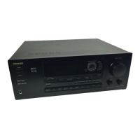
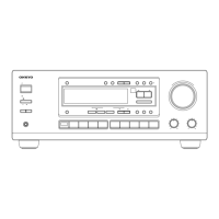
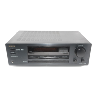
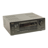
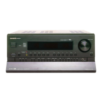
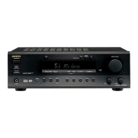
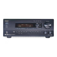
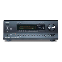
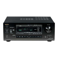
TX-DS595
MAIN MICROPROCESSOR TERMINAL DESCRIPTIONS
TX-DS595
 Loading...