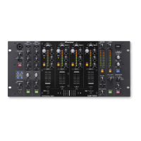
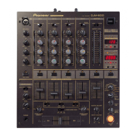
DJM-500
6. IC INFORMATION
. The Information shown in the list is basic information and may
not correspond exactly to that shown in the schematic diagram,
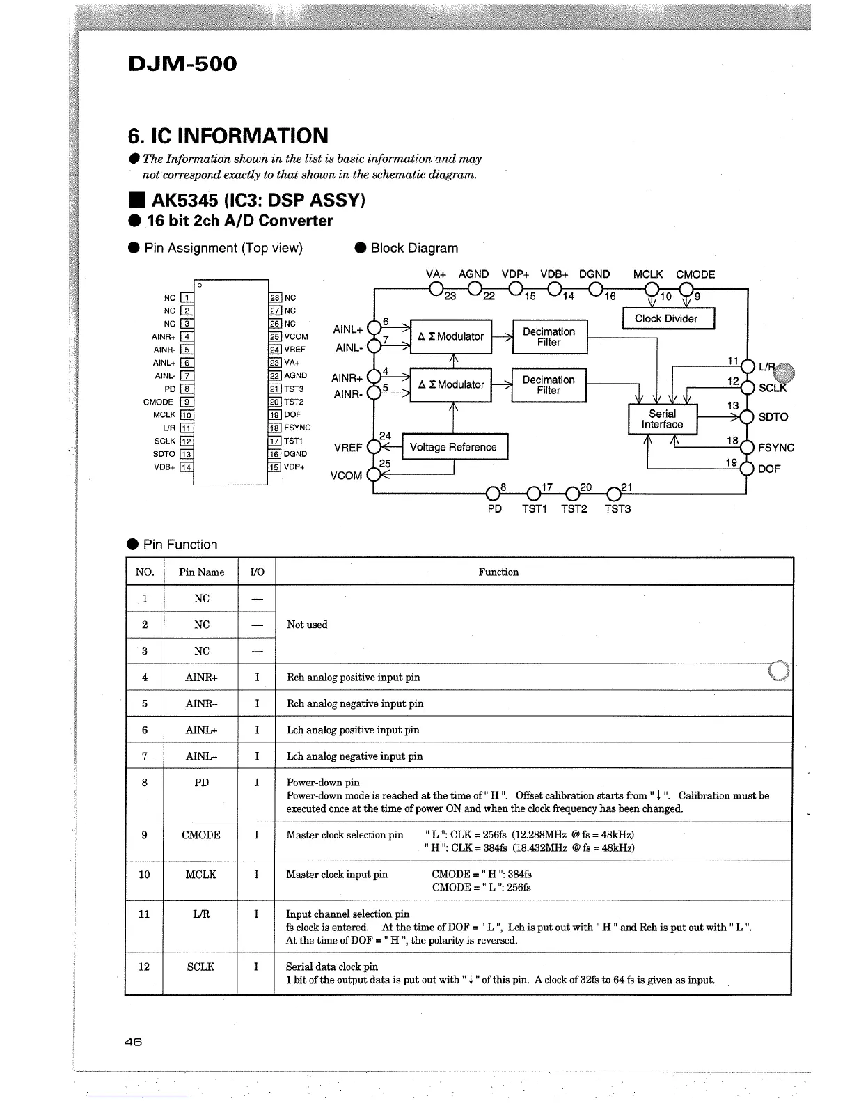
. AK5345 (lC3: DSP ASSY)
. 16 bit 2ch AID Converter
. Pin Assignment (Top view)
o
NC
NC
NC
AINR+
AINR-
AINL+
AINL-
PD
CMODE
MCLK
UR
SCLK
SDTO
VDB+
. Pin Function
. Block Diagram
VA+ AGND VDP+ VDB+ DGND
MCLK CMODE
AINL+
AINL-
FSYNC
DOF
AINR+
AINR-
U
SCL
SDTO
VREF
VCOM
PD TST1 TST2 TST3
NO, Pin
Name
I/O Function
1 NC
-
2
NC
-
Not used
3 NC
-
4 AINR+ I Rch analog positive input pin
~J
5
AINR- I Rch analog negative input pin
6 AINL+ I Lch analog positive input pin
7 AINL- I Lch analog negative input pin
8 PD
I Power-down pin
Power-down mode is reached at the time of" H", Offset calibration star from" l", Calibration must be
executed once at the time of power ON and when the clock frequency has been changed,
9 CMODE I
Master clock selection pin " L ": CLK = 256fs (12,288MHz cg fs = 48kH)
" H ": CLK = 384fs (18.432MH cg fs = 48kH)
10 MCLK I
Master clock input pin CMODE = " H ": 384fs
CMODE = " L ": 256fs
11 lÆ I
Input chanel selection pin
fs clock is entered,
At the time ofDOF =" L", Lch is put out with" H" and Rch is put out with" L",
At the tie ofDOF =" H", the polarty is reversed,
12 SCLK
I
Serial data clock pin
1 bit of the output data is put out with" l " of this pin. A clock of 32fs to 64 fs is given as input,
48
 Loading...