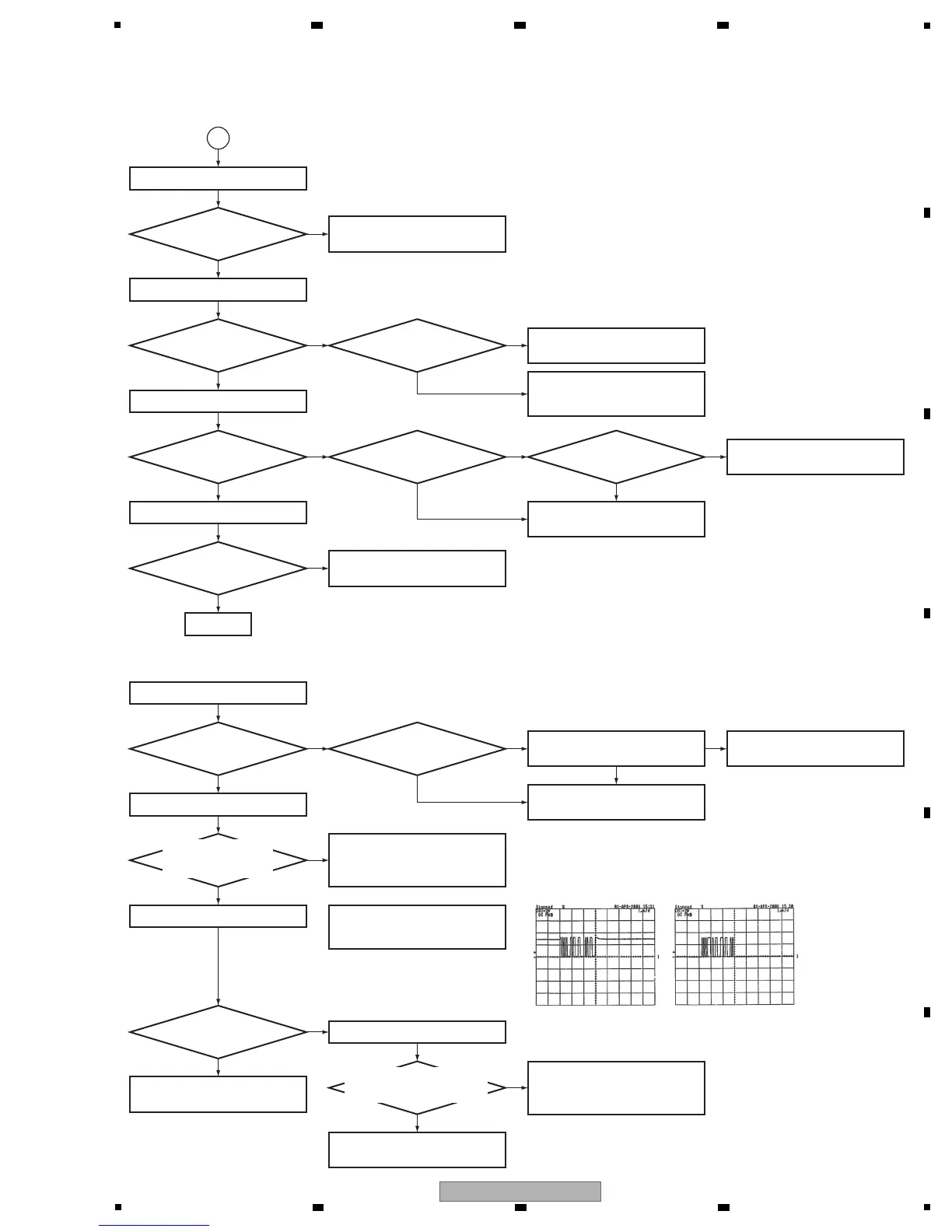
Is the voltage 5 V?
Is the voltage 1.8 V output?
Is REG1 abnomally hot?
Is pin 4 (en) of IC805 low?
Ye s
Ye s
No
No
5 V input
1.8 V output
The output and GND may be
short-circuited. Check the path
between them.
REG1 (pin 3)
REG1 (pin 2)
Ye s
Is the voltage 5 V input?
Is the voltage 5 V output?
No
Is pin 8 (fault) of IC805 high?
No
Ye s
Ye s
Ye s
Ye s
Ye s
OK
Ye s
Ye sYe s
5 V input
IC805 (pins 2, 3)
USB bus power
IC805 (pins 6, 7)
Check the pattern in the path.
No
Check the parts and pattern in the
path of CN801.
No
DATA and ADDRESS lines
between SDRAM (IC803),
FLASH ROM (IC802), and IC801
are may not be connected.
Check the CN704B of CPU Assy
and CN704A of FRONT Assy.
Check the parts and pattern in the
path. Replace XTAL1, etc..
Operation of IC801 is OK.
Go to step 3.
Operation of IC801 is OK.
Go to step 3.
D+ and D- should have waveform
during normal condition. Check the
pattern in the path of IC801. etc..
No
Check the pattern in the path.
No
Replace REG1.
Replace IC805.
D
To Step 2
Step 2: Operation of USB Media Control IC
IC801 (pins 54, 55)
CN802 usb_rx,tx (pins 4, 5)
Ye s
JACK801 (pins 2, 3)
IC801 (pin 44) -> IC803 (pin 38)
Is there a 12 MHz output?
CP803 pins 1, 2 (reset,rdy)
is high?
Are there the waveforms
like figure?
After turning the power on and
several seconds later,does SDCLK
change 12 MHz to 80 MHz?
No
No
No
usb_rx and usb_tx should be high
during operation. Check the
pattern in the path of FRONT and
CPU Assys.
No
Check the path to CPU Assy.
NG
xin/xout
initial communication [SDCLK]
Do usb_rx and usb_tx
communication
with main micom?
Fig. D+
X: 1 μS/div, Y: 2 V/div
X: 1 μS/div, Y: 2 V/div
Fig. D-
 Loading...