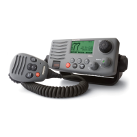
4.3.1 PLL (Phase Lock Loop Circuit)
The PLL circuit is the frequency synthesizer in the VHF5200.
The reference frequency of 12.8 MHz is provided by crystal
XTLI
and IC3. IC3 contains the
reference oscillator (12.8 MHz) circuit, the phase comparator, the program counter and the
phase detector. The 12.8 MHz reference signal is divided by 512 in the program counter in IC3
to obtain a 25 KHz reference signal. The dividing ratio is determined by CPU
IC201.
The VCO
output from oscillator Q4 is amplified by buffer amplifier Q3, and returned to IC3 and is divided
by the dividing ratio N to obtain a 25 KHz signal. N for 1 N in lC3 is determined by CPU
IC201.
Both of these
25KHz
signals are fed into the phase comparator circuit of IC3.
The phase detected signal, obtained by comparing the phase difference between these two
signals, is applied to LPF between pins 11 and 12 of IC4 to get a DC voltage correlated with the
phase difference.
The DC voltage acts on the VCO to make the two 25 KHz signals the same phase. When this
condition is met, the PLL circuit is locked. If the two signals have a large phase difference, the
PLL is unlocked. In this condition, the unlocked signal is fed to CPU IC201 from lC3 and the
transmitter is compelled to stop.
The VCO output from Q4 is fed to the TX amplifier Q2 and the first RX mixer
Ql9
through
buffer amplifier Q3.
4.3.2 Transmitter Circuit
A signal from the microphone is fed to a pre-emphasis operations amplifier IC3, and modulates
VCO(Q4) through active LPF IC2.
The VCO output signal from Q4 is sent to the RF power amplifiers ICI,
Ql
and Q2 through
buffer amplifier Q3. The RF signal from ICI is fed to the antenna through a low pass titter.
The DC voltage correlative to the RF output is detected by
02
and Q9. amplified by Q24 and
fed to ICI .The output voltage from ICI controls the RF power to keep the RF output at a con
stant level.
4.3.3 Receiver Circuit
1) RF Circiut
The signal from the antenna passes through the single tuned band pass filter, and is amplified by RF
amplifier Q17, and is fed into a triple tuned band pass filter. The signal is then mixed by
Q19
(first mixer) and produces the first IF signal of 21.6 MHz. This signal is sent to a crystal filter
(21.6 MHz) and first IF amplifier Q20, mixed by IC4 , the second mixer, and becomes an
audio signal after detection.
2) IF Circuit
The output of the first IF amplifer Q20 is fed into IC4. IC4 contains the second mixer, second
local oscillator, 455KHz amplifer, quadrature detector and DC switching amplifer.
A455 KHz ceramic filter is installed between pins 3 and 5 of IC4 to examine the selectivity of
this unit.
The detector output is separated into audio and noise components by an RC filter. The noise
component is fed back to the noise amplifer section of 164. Its output is rectified by a diode
in IC4 and then fed to the switching amplifer in IC4.
3) AF Circuit
The AF signal from IC4 is amplified by IC5 to drive the speaker while the receiver is in the
squelched condition. Muting control of IC5 is carried out by the CPU IC 201.
4) Weather Alert Tone Detecting Circuit
If a weather alert tone is included in the AF signal from IC4 while receiving the weather service
broadcast, IC6 detects it and notifies an alert condition to CPU
IC201.
17
 Loading...