Renesas RA Microcontrollers EK-RA6M2 v1 – User's Manual
R20UT4578EU0102 Rev.1.02 Page 25 of 32
Jul.29.20
5.5.4 Pin Header J4
Pin header J4 is a 2-column by 20-row through-hole pin header on 2.54 mm centers.
Table 16. Pin Header J4 Pin Assignment
Color Key
Secondary Fixed Function pins
*Note: The RA6M2 MCU does not support the SDHI WP signal, so J4-24 has been assigned a GPIO signal.
5.6 Additional Features
5.6.1 Analog Reference Voltages
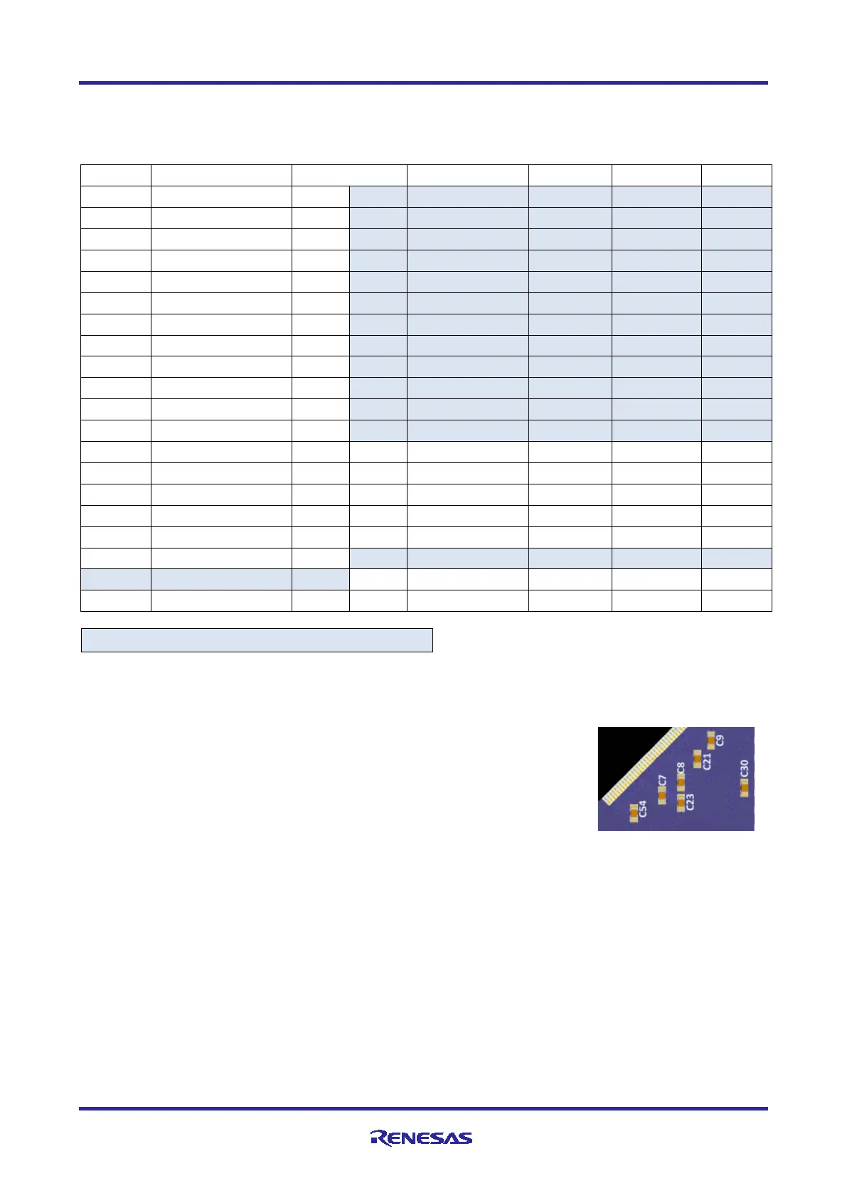
Footprints for installation of capacitors C21 and C23 are provided on the board.
These two capacitors provide noise-bypass capability for ports P010/P011 and
for ports P012/P013. See Figure 24 for the circuit design.
Port pair P010/P011 may be assigned as GPIO, where bypass capacitor C21
would damage signal quality. When P010/P011 are to be assigned as VREFH0/VREFL0, installation of the
capacitor C21 can reduce reference voltage noise and improve ADC measurement and DAC output quality.
The Evaluation Kit Board was designed for Samsung P/N CL10B104KB8NNNC, or similar, noise-bypass
capacitors.
Port pair P012/P013 may be assigned as GPIO, where bypass capacitor C23 would damage signal quality.
When P012/P013 are to be assigned as VREFH/VREFL, installation of capacitor C23 may reduce reference
voltage noise and improve ADC measurement and DAC output quality. The EK-RA6M2 was designed for
Samsung P/N CL10B104KB8NNNC, or similar, noise-bypass capacitors.

 Loading...


