LC-32/40/46LE600E/RU/S (1st Edition)
6 – 24
2.19. IC9611 (VHiTCR5SB25-1Y)
2.19.1 Pin Connections and short description
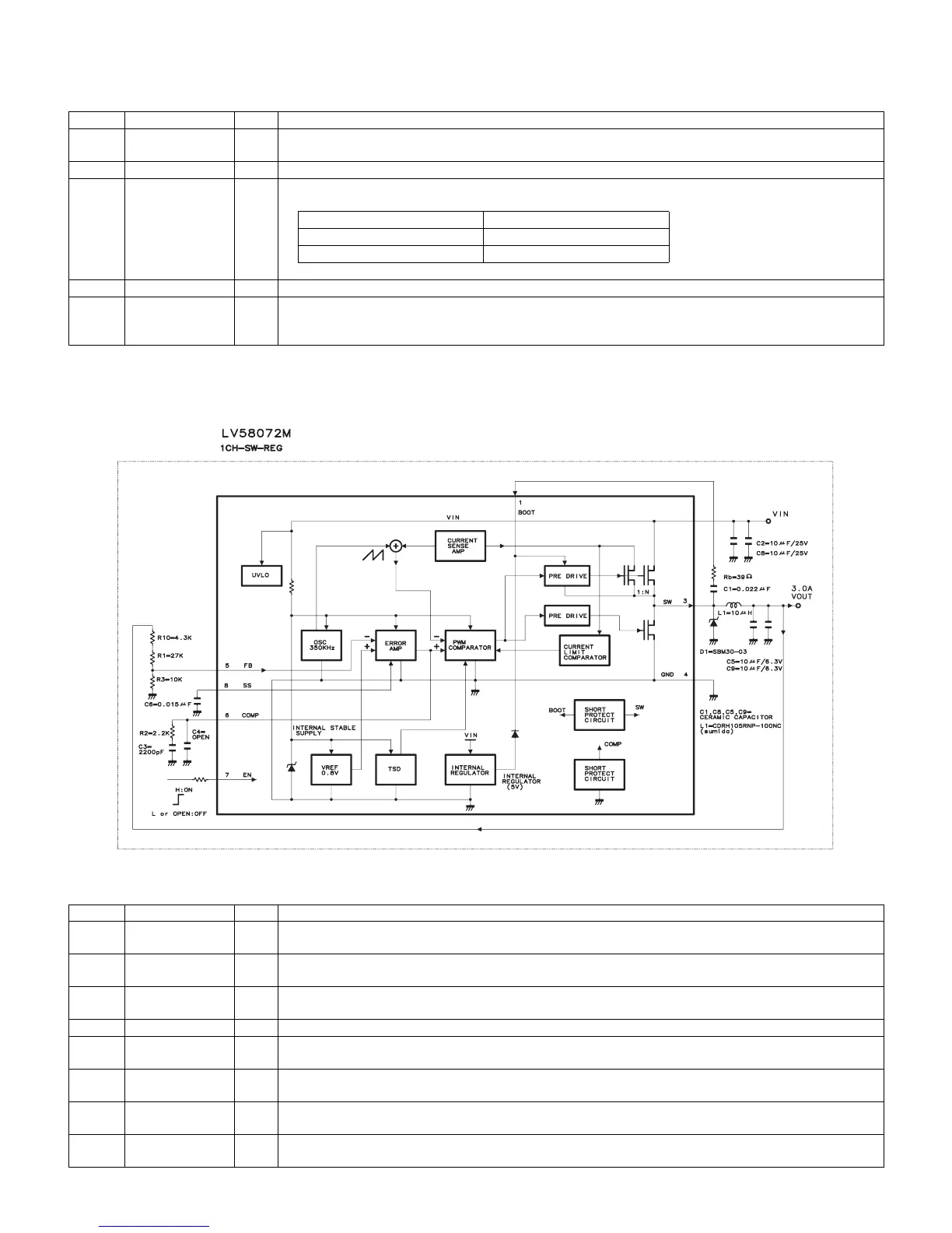
2.20. IC9604 (VHiLV58072M-1Y)
2.20.1 Block Diagram
2.20.2 Pin Connections and short description
Pin No. Pin Name I/O Pin Function
1 VIN I Input power source terminal.
A small, ceramic type can be used for the input capacitor (0.1µF).
2 GND — Ground
3 CONTROL I Control terminal. In control voltage ON, it is 1.5-6V, and turning off is 0.25V or less.
Control voltage Output voltage
HIGH ON
LOW OFF
4 NC — No connection
5 VOUT O Output voltage terminal.
The output voltage of TCR5SB25 is 2.5V±0.05V.
A small, ceramic type can be used for the output capacitor (1.0µF).
Pin No. Pin Name I/O Pin Function
1 BOOT I Bootstrap Terminal
Connect the boost capacity of about 0.022µF between SW terminals.
2 VIN I Input Voltage Terminal
Connect very big capacity between GND.
3 SW O Power Switch Terminal
Connect output LC filter. Moreover connect the above-mentioned capacity between BOOT terminals.
4 GND — Ground
5 FB I Feed Back Terminal
The output voltage is set by the division resistance between the output voltages.
6 COMP I Phase Compensation Terminal
The phase amends external capacity and the resistance of the DC/DC converter close loop are connected.
7 EN I Enable Terminal
The converter works by the High voltage impression.
8 SS — Softstart Terminal
The soft start time is set by built-in 10µA source voltage and external soft start capacity.
 Loading...