4-63
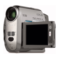
DCR-HC39E/HC41/HC42/HC42E/HC43/HC43E
Board Name
Waveform Parts Location Pattern
(Shown on Page) (Shown on Page) Total Number of Layers Layers Not Indicated
CD-534 4-81 4-89 4 layers 2 to 3 layers
PD-238 4-88 4-92 2 layers –
CR-050 – – 2 layers –
SI-042 – 4-92 2 layers –
LB-109 – – 2 layers –
JK-278 – 4-92 2 layers –
MS-249 – – 2 layers –
FP-180 Flexible – – 1 layer –
FP-186 Flexible – – 1 layer –
FP-187 Flexible – – 1 layer –
FP-826 Flexible – – 1 layer –
FP-467 Flexible – – 1 layer –
FP-228 Flexible – – 1 layer –
4-3. PRINTED WIRING BOARDS
4-3. PRINTED WIRING BOARDS
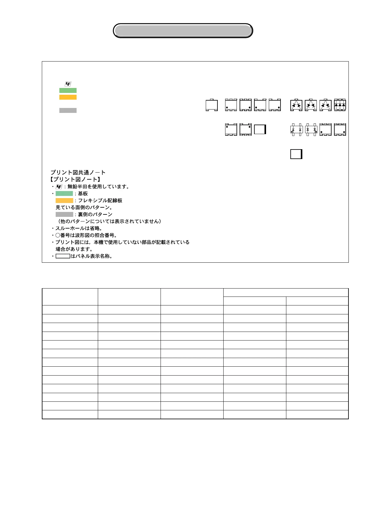
• : Uses unleaded solder.
•
: Circuit board
: Flexible board
Pattern from the side which enables seeing.
: pattern of the rear side
(The other layers’ patterns are not indicated)
• Through hole is omitted.
• Circled numbers refer to waveforms.
• There are a few cases that the part printed on diagram
isn’t mounted in this model.
• C: panel designation
(ENGLISH)
THIS NOTE IS COMMON FOR PRINTED WIRING BOARDS
4-3. PRINTED WIRING BOARDS
(JAPANESE)
BOARD INFORMATION
21
3
21
3
21
3
345
21
123
654
EB
C
31
5
2
46
123
654
31
5
2
46
123
54
43
12
312
45
534
12
14
23
46
2
5
31
12
4
3
14
23
• Chip parts.
Transistor Diode
 Loading...