HBD-TZ215/TZ715
HBD-TZ215/TZ715
2727
For Schematic Diagrams.
Note:
• All capacitors are in μF unless otherwise noted. (p: pF) 50
WV or less are not indicated except for electrolytics and
tantalums.
• All resistors are in Ω and 1/4 W or less unless otherwise
specifi ed.
•
f
: internal component.
• C : panel designation.
THIS NOTE IS COMMON FOR PRINTED WIRING BOARDS AND SCHEMATIC DIAGRAMS.
(In addition to this, the necessary note is printed in each block.)
• A : B+ Line.
• B : B– Line.
• Voltages and waveforms are dc with respect to ground
under no-signal conditions.
no mark
: TUNER (FM)
< > : DVD PLAY
*
: Impossible to measure
• Voltages are taken with VOM (Input impedance 10 M).
Voltage variations may be noted due to normal production
tolerances.
• Waveforms are taken with a oscilloscope.
Voltage variations may be noted due to normal production
tolerances.
• Circled numbers refer to waveforms.
• Signal path.
F : TUNER
J : DVD PLAY
d : USB
f : AUDIO IN
L : VIDEO
• Abbreviation
E3 : Middle East & African models
E12 : Indian model
E32 : Latin American model
For Printed Wiring Boards.
Note:
• X : Parts extracted from the component side.
• Y : Parts extracted from the conductor side.
•
f
: Internal component.
• : Pattern from the side which enables seeing.
(The other layers' patterns are not indicated.)
• Indication of transistor.
C
B
These are omitted.
E
Q
B
These are omitted.
CE
Q
• MAIN board is multi-layer printed board. However, the
patterns of intermediate-layers have not been included in
this diagrams.
• Circuit Boards Location
Caution:
Pattern face side:
(SIDE B)
Parts face side:
(SIDE A)
Parts on the pattern face side seen
from the pattern face are indicated.
Parts on the parts face side seen from
the parts face are indicated.
Note: The components identifi ed by mark 0 or dotted
line with mark 0 are critical for safety.
Replace only with part number specifi ed.
MAIN board
POWER board
MS-203 board
TUNER (FM)
KEY-SW board
FL board
USB KEY board
P-SW board
KZ-USB board
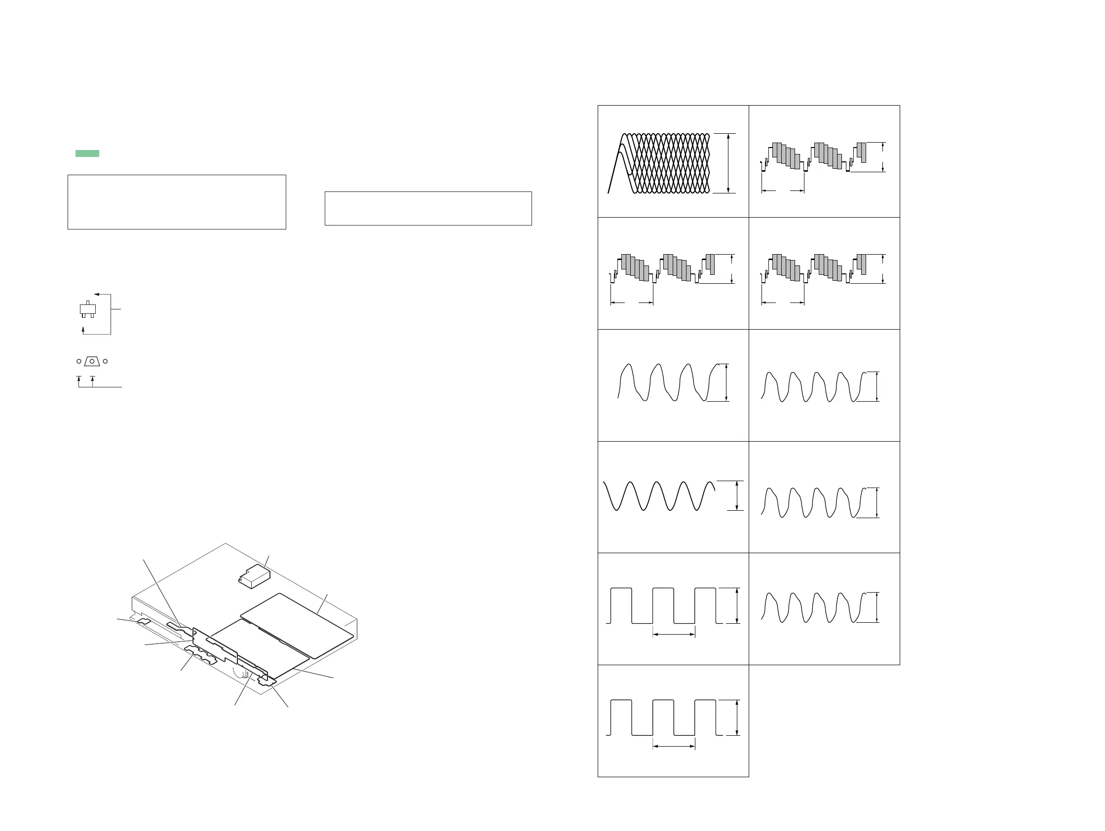
• Waveforms
– MAIN Board –
1 V/DIV, 10 ns/DIV
1 IC1101 0 (DVDRFIP)
2 IC1101 <z,m (CVBS)
7 IC400 4 (IN2)
8 IC400 2 (OUT)
3 IC1101 <xc, (XTALO)
4 IC503 qd (Xout)
5 IC404 7 (LRCK)
6 IC404 8 (BCK)
9 IC3007 4 (Y)
q; IC3005 rk (XFSOIN)
qa IC3005 qf (XFSOOUT)
100 mV/DIV, 100 ns/DIV
500 mV/DIV, 20 Ps/DIV
500 mV/DIV, 20 ns/DIV
1 V/DIV, 100 ns/DIV
1 V/DIV, 10 Ps/DIV
1 V/DIV, 0.1 Ps/DIV
1 V/DIV, 10 ns/DIV
1 V/DIV, 10 ns/DIV
H
1.3 Vp-p
500 mV/DIV, 20 Ps/DIV
H
1.3 Vp-p
1 V/DIV, 20 Ps/DIV
H
2.6 Vp-p
1.6 Vp-p
27 MHz
540 mVp-p
3.4 Vp-p
5 MHz
3.2 Vp-p
20.8 Psec
3.2 Vp-p
0.326 Psec
4.8 Vp-p
4.2 Vp-p
4 Vp-p
49.152 MHz
49.152 MHz
49.152 MHz
 Loading...