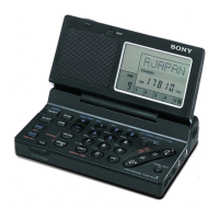
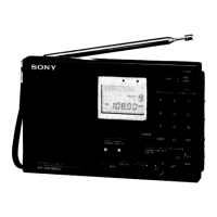
ICF-SW100E/SW100S
– 13 – – 14 –
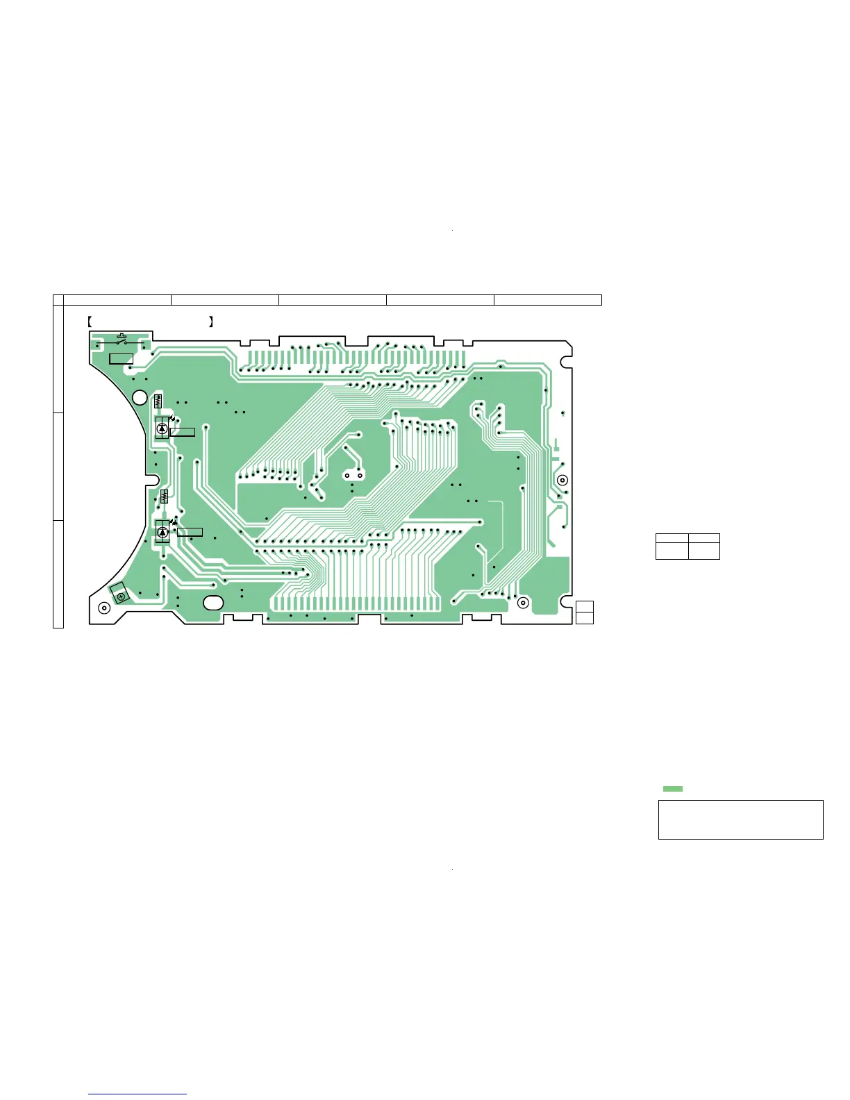
1-5. PRINTED WIRING BOARD – MICROCOMPUTER BOARD (SIDE A) –
MICROCOMPUTER BOARD (SIDE A)
17
(17)
1-651-254-
R605
R604
D604
D605
BT601
S601
LIGHT
LIGHT
LIGHT
2
3 4 5
A
1
B
C
Note on Printed Wiring Boards:
• X : parts extracted from the component side.
• x : parts extracted from the conductor side.
• z : Through hole.
• : Pattern from the side which enables seeing.
(The other layers´ Patterns are not indicated.)
Caution:
Pattern face side: Parts on the pattern face side seen from the
(Side A) pattern face are indicated.
Parts face side: Parts on the parts face side seen from the
(Side B) parts face are indicated.
Ref. No. Location
• Semiconductor
Location
D604 B-1
D605 C-1
 Loading...