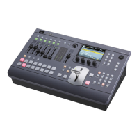
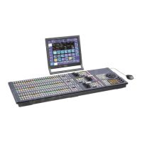
1-7-3. Audio Signal Processing Circuit
The analog audio input connector has eight channels in total, including 6-channel balanced signal input (XLR type x 2
+ TRS type x 4) and 2-channel unbalanced signal input (phone jack).
The analog audio output connector has nine channels in total , including 6-channel balanced signal output (XLR type x
2 + TRS type x 4), 2-channel unbalanced signal output (phone jack), and a single-channel stereo output (TRS-type
stereo).
Analog audio input signals are converted to digital audio signals by the A/D converter (IC102, IC302) on the CN-3403
board, and the digital audio signals are sent to the Audio Matrix FPGA (IC5005) on the MIX-54 board. The digital video
embedded audio signals that are output from the FPGAs (IC5001, IC5002) are converted to 8- stereo signals by the
sampling rate converter (IC3208 to IC3215). Then the 8- stereo signals are input to the Audio Matrix FPGA (IC5005).
A The Audio Matrix FPGA selects 6-stereo signals from signals from the analog audio input connector and signals from
the sampling rate converter (IC3208 to IC3215), and then sends the 6-stereo signals to the DSP (IC5105).
The DSP (IC5105) adjusts gain, mixes signals, and performs delay processing using the SDRAM (IC5104) as a buffer.
The DSP (IC5105) processing result is returned to the Audio Matrix FPGA (IC5005) and is sent to the output circuit on
the CN-3403 board. The 4-stereo embedded audio signals are sent to the Video Mix FPGA (IC5003).
In the CN-3403 board, output digital audio signals are converted to analog audio signals, and the analog audio signals
are output from the analog audio output connector through the buffer amplifier.
Processing commands to the DSP (IC5105) are executed through the S-RAM (IC5000) connected to the CPU bus.
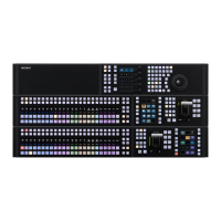
1-7-4. Control Circuit
The MCS-8M controls entire control system with a single-chip CPU (IC10). This circuit has a 2-Mbyte boot flash
memory (IC1201) for booting, a 64-Mbyte flash memory (IC1200) for storing application programs, and a 128-Mbyte
work SDRAM (IC200 to IC203).
The 2-Mbyte boot flash memory (IC1201) contains VxWorks and the 64-Mbyte flash memory (IC1200) contains
application programs. However, 2 Mbytes out of 64 Mbytes of the application flash memory is used for backup of the
boot flash memory. Thanks to this backup system, if the unit cannot be started from the 2-Mbyte boot flash memory
(IC1201) for some reason, the unit can be started from the 64-Mbyte flash memory (IC1200).
The RS-232C serial interface for external communication and the RS-232C serial interface for debug are connected
directly to the serial communication module in the CPU chip (IC10).
The PCI bus of the CPU (IC10) is connected to the USB2.0 controller chip (IC800), and USB signals are sent to the
USB connector (CN101) on the KY-671 board through the USB2.0 hub (IC1301) on the same board. The USB2.0 hub
(IC1301) compensates signal deterioration caused during relay through the cable.
The CPU interface FPGA (IC5004) is connected to the CPU bus. This FPGA contains an image processor (IC6) interface,
an I2C control circuit, a TALLY/GPI control PIO, a fan control circuit, and a circuit for controlling button s, LCD,
LEDs, and fader on the panel.
Control signals to the devices on the panel are integrated to a serial differential signal (LVDS) by the channel link (IC900,
IC200), and the LVDS signal is sent to the devices.
Information of the button, potentiometer, XY-Pointer, and fader from the panel is also integrated to a serial signal in
the KY-671 board, and the serial signal is sent to the MIX-54 board.
The frame memory interface in the video signal processing block, the DSP interface SRAM in the audio block, and the
Audio Matrix FPGA register are connected to the CPU local bus.
Variable resistance values of the fader lever for audio mixer and transition, potentiometer value for audio monitor output
adjustment, and X-Y pointer output value on the panel are converted to digital values by the A/D converter (IC401,
IC402), and the digital values are sent to the CPU interface FPGA (IC5004) as a serial signal.
Indication of the LEDs is controlled by parallel signals converted from a serial signal by the shift register.
MCS-8M
1-37
 Loading...