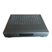
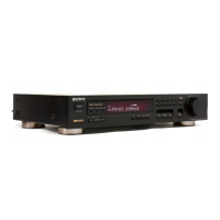
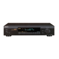
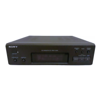
ST-EX880/MS717
– 25 – – 26 –
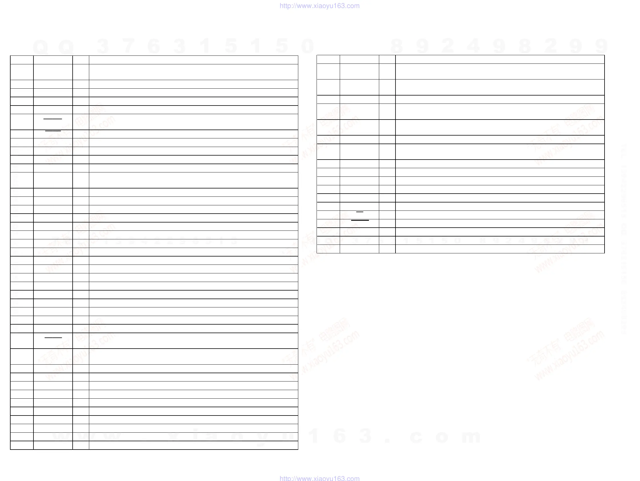
5-12. IC PIN FUNCTION DESCRIPTION
• MAIN BOARD IC201 µPD78016FGC-544-AB8 (SYSTEM CONTROLLER)
Pin No. Pin Name I/O Function
1 to 4
DATA 0 to
DATA 3
I/O
Two-way data bus with the system control bus
5 IF+50 I
Fixed at “L” in this set
6 IF–50 O
Fixed at “L” in this set
7, 8 GND —
Ground terminal
9 VSS —
Ground terminal
10 POWER O
Power on/off control signal output for the +10V and +5V power supply
“L”: power on, “H”: standby
11 MUTE O
Tuner muting on/off control signal output terminal “L”: muting on
12 AC RELAY O
Relay drive signal output for the AC on/off control “L”: standby, “H”: power on
13, 14 NC O
Not used (open)
15
AM MONO O
AM forced monaural control signal output terminal “H”: forced monaural Not used (open)
16 AM/FM O
FM/AM selection signal output terminal Not used (open)
17 IFNG O
Intermediate frequency count effect signal output terminal “L”: NG, “H”: OK
Not used (open)
18 STEREO I
Stereo detection signal input from the LA1835 (IC1) “L”: stereo
19 SIGNAL I
FM/AM frequency detection signal input from the LA1835 (IC1) “L”: tuned, “H”: detuned
20 DATA IN I
PLL serial data input from the FM/AM PLL (IC51)
21 DATA OUT O
PLL serial data output to the FM/AM PLL (IC51)
22 CLOCK O
PLL serial data transfer clock signal output to the FM/AM PLL (IC51)
23 CE O
PLL serial chip enable signal output to the FM/AM PLL (IC51)
24 VSS —
Ground terminal
25 SIRCS IN I
Sircs remote control signal input from the remote control receiver (IC902)
26 STAND BY O
LED drive signal output for the STANDBY indicator Not used (open)
27 ONCE O
LED drive signal output for the ONCE indicator (D905) “L”: LED on
28 DAILY O
LED drive signal output for the DAILY indicator (D904) “L”: LED on
29 REC O
LED drive signal output for the REC indicator (D903) “L”: LED on
30 SLEEP O
LED drive signal output for the SLEEP indicator (D902) “L”: LED on
31
ENCORDER IN A
I
Jog dial pulse (A) input from the rotary encoder (S915) (for MULTI CONTROLLER)
32
ENCORDER IN B
I
Jog dial pulse (B) input from the rotary encoder (S915) (for MULTI CONTROLLER)
33 AUBUS IN I
Sircs remote control signal input for the audio bus
34 AUBUS OUT O
Sircs remote control signal output for the audio bus
35 RESET I
System reset signal input from the reset signal generator circuit “L”: reset
For several hundreds msec. after the power supply rises, “L” is input, then it changes to “H”
36 RDS CLK I
Serial data transfer clock signal input from the RDS decoder (IC302)
Used for the ST-EX880 (ST-MS717: fixed at “L”)
37 CLOCK I/O
Bus data transfer/reading clock signal in/out terminal for the system control bus
38 BUSY I/O
Busy signal in/out terminal for the system control bus
39 AC OFF I AC off detection signal input terminal “L”: AC off
40 VDD —
Power supply terminal (+5V)
41 X2 O
Main system clock output terminal (10 MHz)
42 X1 I
Main system clock input terminal (10 MHz)
43 GND IC (VPP) —
Ground terminal
44 XT2 O
Sub system clock output terminal (32.768 kHz)
45 XT1 I
Sub system clock input terminal (32.768 kHz)
46 AVSS —
Ground terminal (for A/D converter)
Pin No. Pin Name I/O Function
47 KEY IN 1 I
Key input terminal (A/D input) (S907 to S913)
ONCE, DAILY, REC, SLEEP, CLOCK/TIMER SET, ENTER/YES, MENU/NO keys input
48 KEY IN 2 I
Key input terminal (A/D input) (S901 to S906)
STEREO/MONO, BAND, PRESET, MANUAL, AUTO, DISPLAY keys input
49 KEY IN 3 I
Key input terminal (A/D input) (S914) I/u (power) key input
50 RDS DATA I
Serial data input from the RDS decoder (IC302)
Used for the ST-EX880 (ST-MS717: fixed at “L”)
51 DESTINATION I
Input terminal for the destination setting
(Tourist model: fixed at “L”, Except Tourist model: open)
52 DESTINATION I
Input terminal for the destination setting (fixed at “L”)
53 DESTINATION I
Input terminal for the destination setting
(Tourist model: open, Except Tourist model: fixed at “L”)
54 DESTINATION I
Input terminal for the destination setting (ST-EX880: open, ST-MS717: fixed at “L”)
55 AVDD —
Power supply terminal (+5V) (for A/D converter)
56 AVREF I
Reference voltage (+5V) input terminal (for A/D converter)
57 GND —
Ground terminal
58 SDATA O
Serial data output to the fluorescent indicator tube driver (IC901)
59 SCK O
Serial data transfer clock signal output to the fluorescent indicator tube driver (IC901)
60 CS O
Chip select signal output to the fluorescent indicator tube driver (IC901) “L” active
61 RESET O
Reset signal output to the fluorescent indicator tube driver (IC901) “L”: reset
62 ERRORS O
Output terminal of the error monitor Not used (open)
63 CORRECTION O
Output terminal of the correction monitor Not used (open)
64 RECEIVED O
Output terminal of the receive monitor Not used (open)
w
w
w
.
x
i
a
o
y
u
1
6
3
.
c
o
m
Q
Q
3
7
6
3
1
5
1
5
0
9
9
2
8
9
4
2
9
8
T
E
L
1
3
9
4
2
2
9
6
5
1
3
9
9
2
8
9
4
2
9
8
0
5
1
5
1
3
6
7
3
Q
Q
TEL 13942296513 QQ 376315150 892498299
TEL 13942296513 QQ 376315150 892498299
http://www.xiaoyu163.com
http://www.xiaoyu163.com
 Loading...