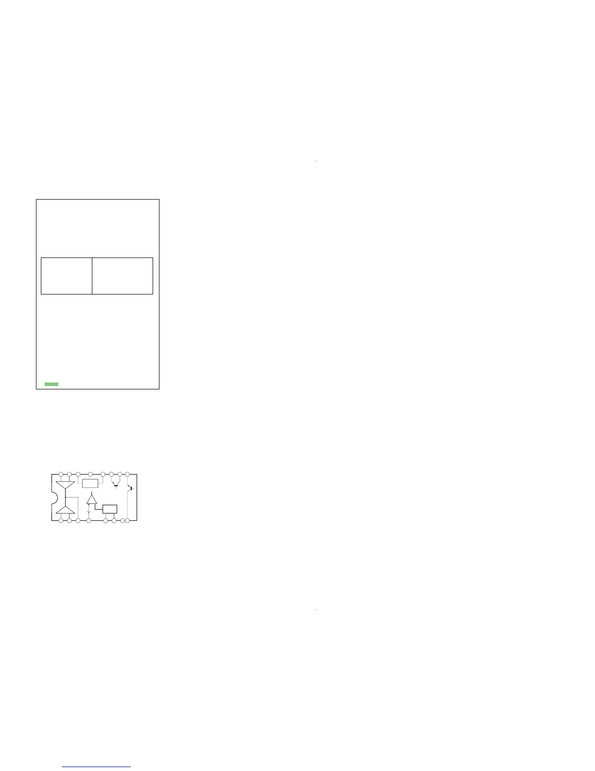
77
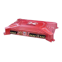
XM-504Z
IC901 µPC494GS
16 15 14 13 12 11 10 9
1 2 3 4 5 6 7 8
OSC
REF. REG.
ERROR
ERROR
0.1V
3-1. IC BLOCK DIAGRAM
THIS NOTE IS COMMON FOR PRINTED WIRING
BOARDS AND SCHEMATIC DIAGRAMS.
(In addition to this, the necessary note is
printed in each block.)
for schematic diagram:
• All capacitors are in µF unless otherwise noted. pF: µµF
50 WV or less are not indicated except for electrolytics
and tantalums.
• All resistors are in Ω and
1
/
4
W or less unless otherwise
specified.
• A : B+ Line.
• B : B– Line.
• Power voltage is dc 14.4V and fed with regulated dc power
supply from +12V and REM terminals.
•Voltage is dc with respect to ground under no-signal
condition.
•Voltages are taken with a VOM (Input impedance 10 MΩ).
Voltage variations may be noted due to normal produc-
tion tolerances.
•Waveforms are taken with a oscilloscope.
Voltage variations may be noted due to normal produc-
tion tolerances.
• Circled numbers refer to waveforms.
• Signal path.
F : AUDIO
for printed wiring boards:
• : Pattern from the side which enables seeing.
Note:
The components identi-
fied by mark 0 or dotted
line with mark 0 are criti-
cal for safety.
Replace only with part
number specified.
Note:
Les composants identifiés par
une marque 0 sont critiques
pour la sécurité.
Ne les remplacer que par une
piéce portant le numéro
spécifié.
SECTION 3
DIAGRAMS
 Loading...