B2.8
T855 Circuit Operation
M850-00
31/09/98 Copyright TEL
The audio can also be disabled using the "RX-DISABLE" inputs, pads 225 or 228, having
connected the "RX-DISABLE" link between pins 1 & 2 of PL260. An adjustable time
delay (RV220) is provided on these lines. In order to disable the audio, either pad must
be pulled to 0V (refer to Section 1.4 in Part G).
An undedicated relay is provided (RL210) for transmitter keying or other functions and
this can be operated from the mute line by linking PL270.
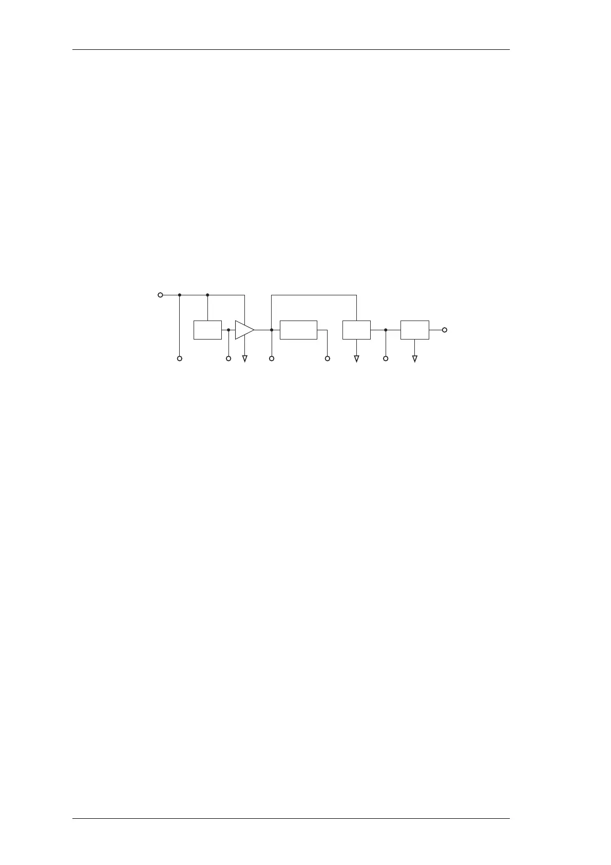
2.8 Power Supply And Regulators
(Refer to the regulators circuit diagram (sheet 6) in Section 6.3.)
Figure 2.4 T855 Power Supply And Regulators Block Diagram
The T855 is designed to operate off a 10.8-16V DC supply (13.8V nominal). A 5.3V regu-
lator (IC630) runs directly from the 13.8V rail, driving much of the synthesiser circuitry.
It is also used as the reference for a DC amplifier (IC640, Q630 & Q620) which provides
a medium current capability 9V supply.
A switching power supply, based on Q670 and Q660, runs off the 9V supply and pro-
vides a low current capability +20V supply. This is used to drive the synthesiser loop
filter (IC740), giving a VCO control voltage of up to 20V.
The 13.8V supply drives both output audio amplifiers without additional regulation. A
separate 5V regulator (IC610) drives the microprocessor and associated digital circuitry.
The output of this regulator is monitored by the Low Voltage Interrupt (LVI) circuit
(IC650).
LVI
LVI
5V
Reg
DC
Amp
Switching
PS
5V Dig
Reg
µP
Reset
13.8V
Nom.
5V 5V Dig9V 20V
13.8V Nom.
From Rear
D-Range 1
 Loading...