B2.12
T855 Circuit Operation
M850-00
31/09/98 Copyright TEL
2.12 Received Signal Strength Indicator (RSSI)
(Refer to the T800-04-0000 RSSI PCB circuit diagram in Section 6.2 and the IF section cir-
cuit diagram (sheet 3) in Section 6.3.)
The RSSI option PCB plugs directly into the main PCB (support circuitry being fitted as
standard). It is fitted to the T855 whenever receiver signal strength monitoring is
required, e.g. trunking or voting. Its function is to provide a DC voltage proportional to
the signal level at the receiver input. The DC voltage is available at D-range 1 (PL100
pin 5).
The RSSI also provides the capability for high level signal strength muting, which may
be selected on PL250 (refer to Section 3.5). The mute threshold may be set between
-115dBm and -70dBm by RV235.
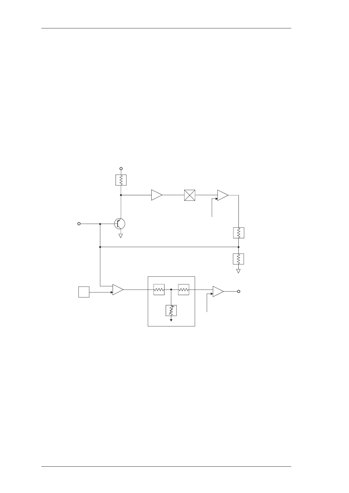
Figure 2.7 T855 RSSI Block Diagram (T800-04-0000 RSSI PCB)
The variable gain stage (Q1A) is a common emitter amplifier with its emitter grounded
and the AGC control loop voltage applied to its base. Since the AGC loop will maintain
a constant signal level at the collector, the gain of Q1 must be proportional to the incom-
ing 455kHz signal level. The gain of Q1 is linearly proportional to its collector current
which itself is exponentially related to the base-emitter voltage. Thus there is a logarith-
mic relationship between the base-emitter voltage and the gain. The circuit therefore
produces a feedback voltage, and an output voltage, logarithmically related to the RF
input signal.
The AGC loop is followed by a DC amplifier which provides level shifting, temperature
compensation and gain to give a nominal 1V/10dB at the RSSI output. RV320 on the
main PCB is used to set the RSSI voltage to a fixed value at a given RF input signal
strength.
+V
Amp Detector Error Amp
Q1C Q1A &
Q1B
VDC
Variable
Gain Stage
Q1E
RSSI
Input
Temp Comp
NTC
DC Amp
(Gain= x33)
Temp
Comp
Q1D
DC Offset
(Ref)
RSSI Output
1V/10dB
 Loading...