Clock Generation
The SP701 board provides an I2C programmable (10 MHz – 810 MHz) Si570 oscillator (U45) to
source the 200 MHz default SYSCLK. The U45 (I2C address 0x5D) I2C02_SYSOSC bus is
connected to U23 TCA9548A main I2C0 bus switch channel 1. The U45 Si570 LVDS output is
connected to FPGA U1 bank 33 MRCC pins AE8 (P) and AE7 (N). See the I2C Bus Topology
secon for U45 programming setup informaon.
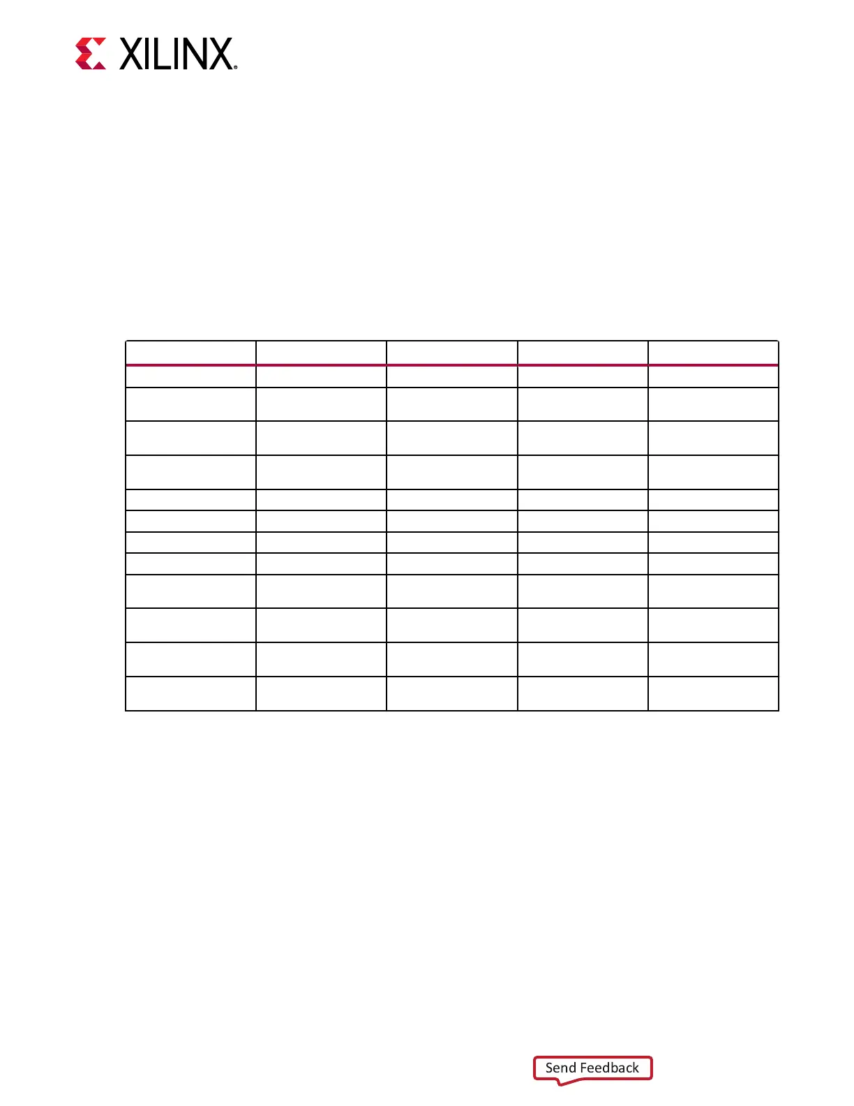
The following table lists the clock types on the SP701 board.
Table 8: SP701 Clocks
Clock Direction Frequency I/O Standard Bank
SYS_CLK
In to FPGA from Si570 33.3333 MHz LVDS Bank 33, MRCC
DDR3L CK
Out from FPGA to
DDR3L
400 MHz - 800 MHz DIFF_SSTL15 Bank 34, DQS
ETH1/2_GTX_CLK
Out from FPGA to
DP83867IR
125 MHz LVCMOS_33 Bank 33, SE I/O
ETH1/2_RX_CLK
In to FPGA from
DP83867IR
125 MHz LVCMOS_25 Bank 33, SRCC/MRCC
MIPI_CSI_CLK
In to FPGA from PCAM 672 MHz LVDS_25 Bank 33, SRCC/MRCC
MIPI_DSI_CLK
Out from FPGA to LCD TBD HSTL_18 Bank 13, Diff I/O
FMC_CLK0_M2C
FMC LPC to FPGA Variable LVDS_25/HSTL_18 Bank 36, MRCC
FMC_CLK1_M2C
FMC LPC to FPGA Variable LVDS_25/HSTL_18 Bank 35, MRCC
FMC_LA00_CC
Out/In by FPGA for
FMC LPC
Variable LVDS_25/HSTL_18 Bank 36, SRCC
FMC_LA01_CC
Out/In by FPGA for
FMC LPC
Variable LVDS_25/HSTL_18 Bank 35, SRCC
6x of PMOD_CLK
Out from FPGA to 6x
PMOD connectors
Variable LVCMOS_33 Bank 16, SE I/O
HDMI_CLK
Out from FPGA to
ADV7511
25 MHz - 165 MHz LVCMOS_33 Bank 15, SE I/O
The detailed FPGA connecons for the clocks described in the table above are documented in
the SP701 board XDC le, referenced in Appendix B: Xilinx Design Constraints. For more Si570
informaon, see the data sheet at the Silicon Laboratories, Inc. website.
The following gure shows the SP701 board clocking diagram.
Chapter 3: Board Component Descriptions
UG1319 (v1.0) July 12, 2019 www.xilinx.com
SP701 Board User Guide 21

 Loading...


