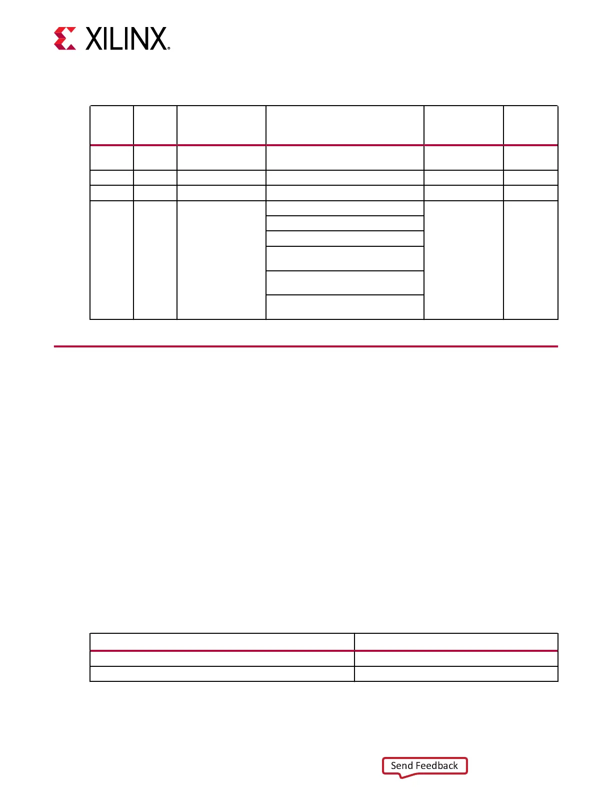
Table 5: Default Switch Settings
Callout Switch Type Function Default
Schematic
Page
Number
15 SW2 5-pole DIP MSP430 U25 GPIO OFF, OFF, OFF, OFF,
OFF
19
21 SW10 8-pole FPGA U1 GPIO All OFF 21
21 SW12 8-pole FPGA U1 GPIO All OFF 21
26 SW13 4-pole DIP
FPGA U1 Configuration:
OFF, ON, OFF=101
OFF
3
Switch OFF = 1 = High; ON = 0 = Low
Mode = SW13[4:2] = Mode[2:0]
JTAG: SW13[4:2] = OFF, ON, OFF =
Mode[101]
MASTER SPI: SW13[4:2] = ON, ON, OFF =
Mode[001]
SW13[1] = INIT_B, OFF = OPEN, ON = 0 =
Low
Spartan-7 Device Configuration
The SP701 board supports two of the 7 series FPGA conguraon modes:
• Master SPI ash memory using the onboard QSPI ash memory
• JTAG
○ J5 micro-AB USB-JTAG interface connector
- USB A-to-micro-B PC to SP701 cable connecon
○ J3 2x7 2 mm keyed JTAG pod at cable header
- Plaorm cable USB II/Parallel cable IV type connecon
Each conguraon interface corresponds to one or more conguraon modes and bus widths as
listed in the following table.
The mode switches M2, M1, and M0 are on SW13 posions 4, 3, and 2, respecvely.
Table 6: SP701 Board FPGA Configuration Modes
Configuration Mode SW13 Switch Settings M[2:0]
Master SPI 001
JTAG (default) 101
See Table 5, callout 26 SW13 for more informaon on the switch posion.
Chapter 2: Board Setup and Configuration
UG1319 (v1.0) July 12, 2019 www.xilinx.com
SP701 Board User Guide 13

 Loading...


