Chapter 1
Introduction
Overview
The SP701 evaluaon board is based on the XC7S100FGGA676 device, a member of the Xilinx
®
7 series FPGA family. It is opmized for low cost, low power, and high I/O performance. It comes
with advanced high-performance FPGA logic based on real6-input look up table (LUT), 36 Kb
dual-port block RAM, support for DDR3L interface up to 1866 Mb/s, XADC with 12-bit
1 MSPA ADC with on-chip thermal and supply sensors, and powerful clock management les
(CMTs). The board is designed for high-performance and lower power with a 28 nm, 1V core
voltage process. For lower power, it has a 0.9V core voltage opon.
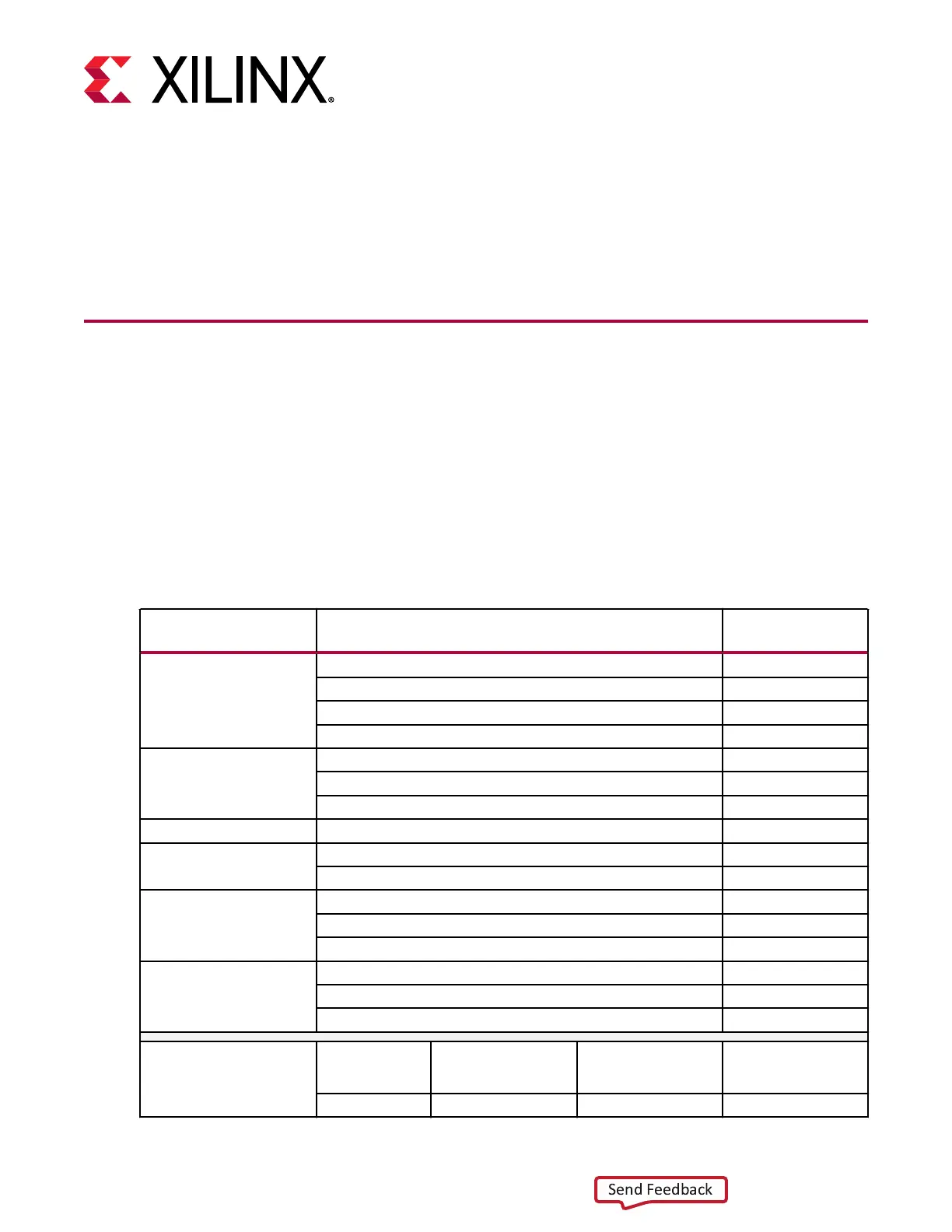
Table 1: XC7S100 Resources
Spartan
®
-7 FPGA
Resources
Component Features
Logic Resources Part Number XCS7100
Logic Cells 102,400
Slices 16,000
CLB Flip-flops 128,000
Memory Resources Max. Distributed RAM (Kb) 1,100
Block RAM/FIFO w/EEC (36 Kb each) 120
Total Block RAM (Kb) 4,320
Clock Resources Clock Mgmt. Tiles (1 MMCM + 1 PLL) 8
I/O Resources Max. Single-Ended I/O Pins 400
Max. Differential I/O Pins 192
Embedded Hard IP
Resources
DSP Slices 160
Analog Mixed Signal (AMS)/XADC 1
Configuration AES/HMAC Blocks 1
Speed Grades Commercial Temp (C) -1, -2
Industrial Temp (I) -1, -2, -1L
Expanded Temp (Q) -1
Package Body Area (mm) Ball Pitch (mm) Available User I/O:
3.3V SelectIO™
technology HR I/O
FGGA676 27 x 27 1.0 400
Chapter 1: Introduction
UG1319 (v1.0) July 12, 2019 www.xilinx.com
SP701 Board User Guide 4

 Loading...


