VCU1525 Acceleration Platform User Guide 29
UG1268 (v1.0) November 13, 2017 www.xilinx.com
Chapter 3: Board Component Descriptions
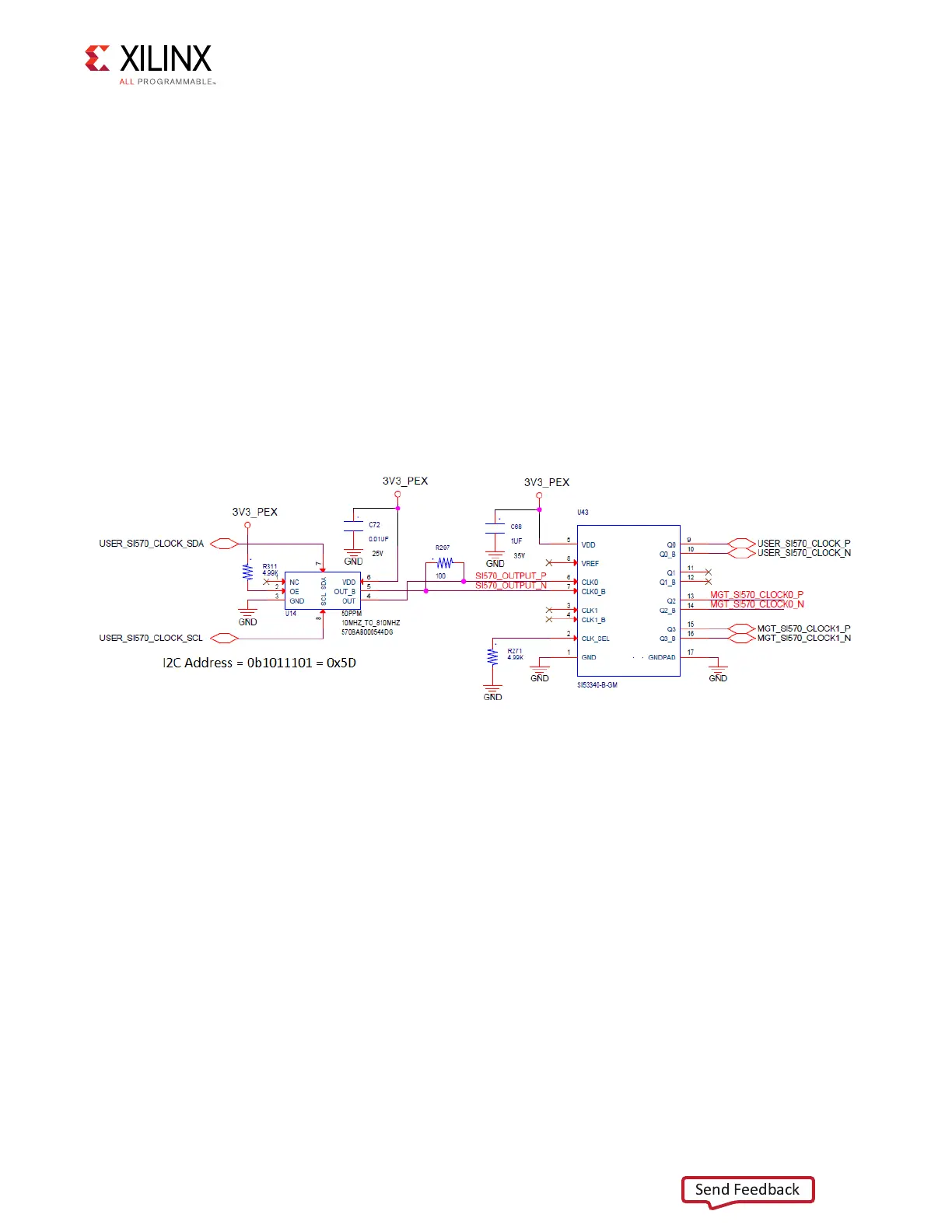
Three of the SI53340 (U14) 1-to-4 LVDS clock buffer outputs are used:
• Q0_P/N: USER_SI570_CLOCK_P/N are wired to GPIO and QSFP0/1 control I/O bank 64
GC input pins AU19 and AV19. The I2C_MAIN_SDA/SCL bus is also wired to bank 64.
•Q1_P/N: Not used.
• Q2_P/N: MGT_SI570_CLOCK0_P/N are AC-coupled to QSFP0 I/F GTY bank 231 REFCLK0
pins M11 and M10.
• Q3_P/N: MGT_SI570_CLOCK1_P/N are AC-coupled to QSFP1 I/F GTY bank 230 REFCLK0
pins T11 and T10.
The FPGA connections for each clock are listed in Appendix A, Master Constraints File
Listing.
The USER_SI570 and QSFP0/1 MGT_SI570 clock circuit is shown in Figure 3-9.
GTY Transceivers
[Figure 2-1, callout 1]
The VCU1525 board provides access to 24 of the 76 GTY transceivers:
• Four GTY transceivers (bank 231) are wired to QSFP28 connector QSFP0 J7.
• Four GTY transceivers (bank 230) are wired to QSFP28 connector QSFP1 J9.
Sixteen GTY transceivers are wired to the PCIe edge connector PEX signals:
• Four GTY transceivers (bank 224) are wired to PCIe edge connector CN1 lanes 15:12.
• Four GTY transceivers (bank 225) are wired to PCIe edge connector CN1 lanes 11:8.
• Four GTY transceivers (bank 226) are wired to PCIe edge connector CN1 lanes 7:4.
X-Ref Target - Figure 3-10
Figure 3-10: USER and MGT SI570 Clock Circuit

 Loading...