VCU1525 Acceleration Platform User Guide 33
UG1268 (v1.0) November 13, 2017 www.xilinx.com
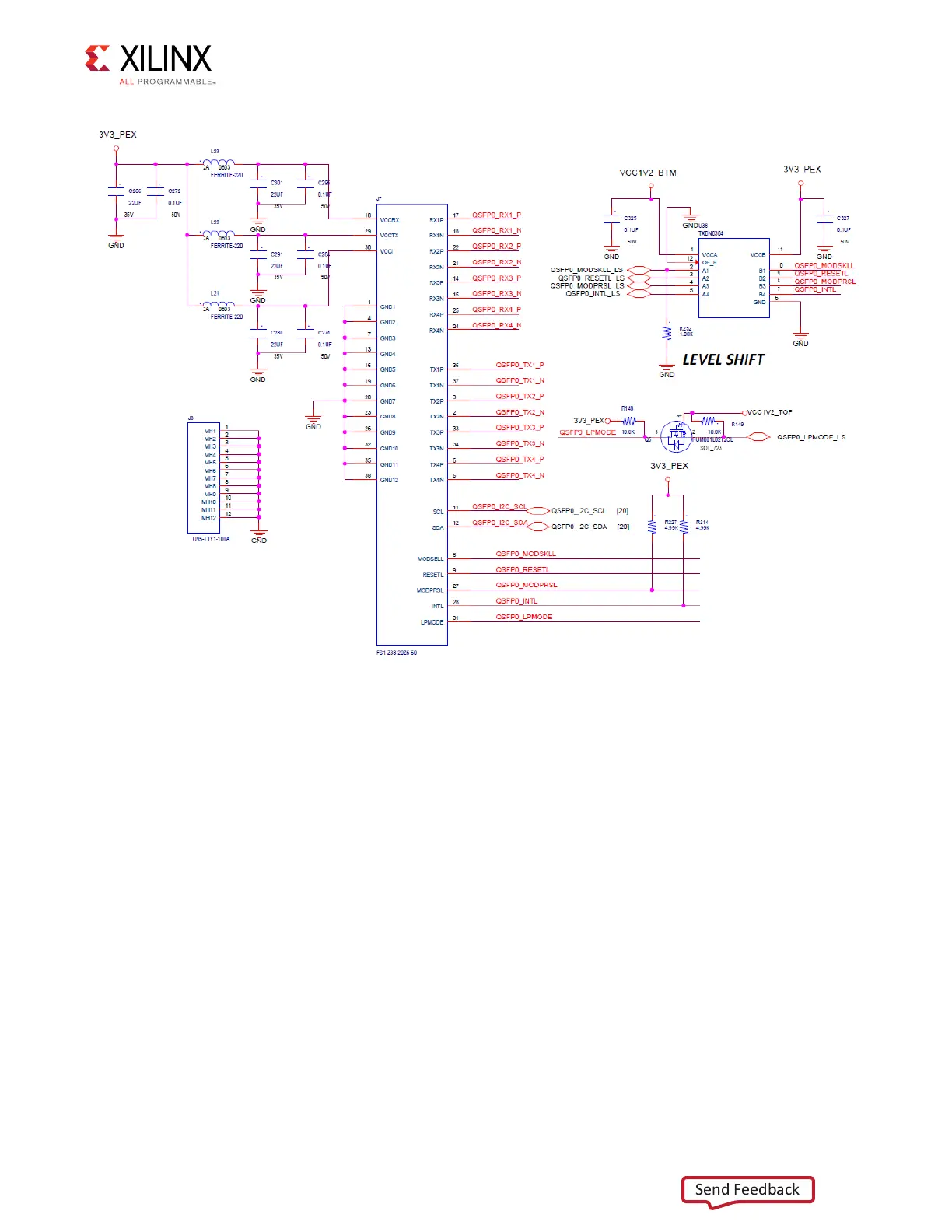
Chapter 3: Board Component Descriptions
The QSFP+ connectors J7 and J9 I2C SCL/SDA are accessible through the TCA9548 I2C
switch U28 IIC_MAIN_SCL/SDA bus. See I2C Bus.
The QSFP+ connectors J7 and J9 I2C control signals are level-shifted by U38/Q5 (QSFP0)
and U48/Q11 (QSFP1) and are connected to FPGA U1 bank 64.
For additional information about the quad small form-factor pluggable (28 Gb/s QSFP+)
module, see the SFF-8663 and SFF-8679 specifications for the 28 Gb/s QSFP+ at the SNIA
Technology Affiliates website [Ref 9].
I2C Bus
The VCU1525 board implements two I2C bus networks, I2C_FPGA_SDA/SCL (4-chan.
PCA9546 U28 at address 0b1110100/0x74) connected to the XCVU9P-L2FSGD2104E U13
only, and I2C_MAIN_SDA/SCL (4-chan. PCA9546 U56 at address 0b1110101/0x75) which is
connected to the MSP432 U19 BMC only.
The TI PCA9546 bus switch can operate at speeds up to 400kHz.
X-Ref Target - Figure 3-12
Figure 3-12: 28 Gb/s QSFP+ Module Connector

 Loading...