16 www.xilinx.com Virtex-5 LXT/SXT/FXT FPGA Prototype Platform
UG229 (v3.0.1) May 21, 2008
Detailed Description
R
3. Configuration Ports
The configuration port header (J17) supports all Virtex-5 device configuration modes. For
use with a Parallel Cable III or Parallel Cable IV cable, the header supports Slave Serial and
JTAG configuration modes.
Table 3 shows Serial mode connectivity between the configuration port header and a
Parallel Cable III or Parallel Cable IV flying-wire cable.
Table 4 shows JTAG mode connectivity between the configuration port header and a
Parallel Cable III or Parallel Cable IV flying-wire cable.
PC4 JTAG Configuration Interface
The JTAG configuration port (J1) for the board allows for device programming and FPGA
debug. This interface can be used with a Parallel Cable III or Parallel Cable IV cable for
JTAG programming and debugging via the JTAG configuration port.
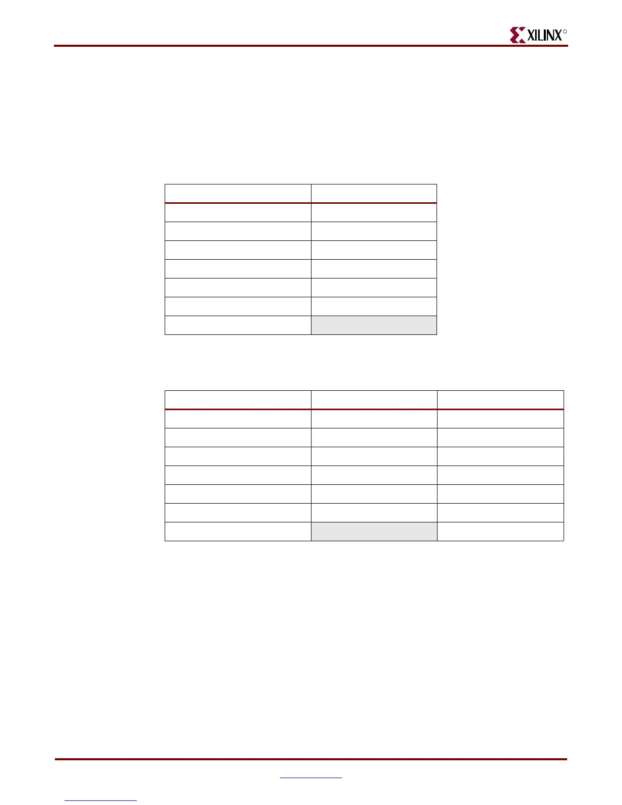
Tabl e 3: Serial Mode
Configuration Port Header Parallel Cable III/IV Pins
VCC3 VCC
GND GND
CCLK CCLK
DONE D/P
DIN DIN
PROG PROG
INIT
Tabl e 4: JTAG Mode
Configuration Port Header Parallel Cable III Pins Parallel Cable IV Pins
VCC3V3 VCC VCC
GND GND GND
TMS TMS TMS
TDI TDI TDI
TDO TDO TDO
TCK TCK TCK
INIT
INIT
 Loading...
