Virtex-5 LXT/SXT/FXT FPGA Prototype Platform www.xilinx.com 25
UG229 (v3.0.1) May 21, 2008
Detailed Description
R
20. SPI Interface
The SPI interface is a four-wire, synchronous serial data bus configuration. The interface
utilizes a 64-Mb STMicroelectronics low-voltage, serial Flash memory device (U10), part
number M25P64, which can be used for FPGA configuration or to hold user data. A SPI
system typically consists of a master device and at least one slave device. For Virtex-5
FPGA configuration, the FPGA is the SPI master and the SPI Flash PROM is the slave
device. The SPI interface uses four signals (Table 12) to communicate between the FPGA
and the Flash PROM device.
The J2 connector allows users to connect a Parallel Cable IV ribbon cable to configure the
SPI device. For SPI programming, refer to the latest version of Xilinx iMPACT software tool
documentation [Ref 6]. To set the Mode pins for SPI configuration, see the Virtex-5 FPGA
Configuration User Guide [Ref 3]. The PROGRAM pin must be held Low when configuring
the SPI device. After configuring the SPI device, the PROGRAM pin must be released to
configure the FPGA from the SPI device.
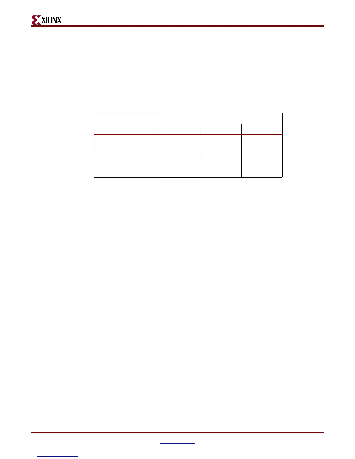
Table 12: SPI Pins
Label
Pin Number For Package Type
FF665 FF1136 FF1738
Serial Clock (C) J11 N15 AH14
Serial Data Out (Q) J10 P15 R15
Chip Select (S_N) Y12 AE14 AL14
Serial Data In (D) AA12 AF14 AM13
 Loading...
