Virtex-5 LXT/SXT/FXT FPGA Prototype Platform www.xilinx.com 21
UG229 (v3.0.1) May 21, 2008
Detailed Description
R
10. Oscillator Sockets
The board has four crystal oscillator sockets (X1, X2, X3, X4), all wired for standard
LVTTL-type oscillators. These sockets connect to the DUT clock pads (Table 6). Onboard
termination resistors can be changed by the user. The oscillator sockets accept both half-
and full-sized oscillators and are powered by the DUT VCCO power supply.
11. Differential Clock Inputs
In addition to the oscillator sockets, there are eight 50Ω SMA connectors (J5, J6, J7, J8, J9,
J10, J11, J12) that allow connection to an external function generator. These connect to the
DUT clock pads (Table 7). They can also be used as differential clock inputs. The
differential clock pairings (differential pairs) are as shown in Table 7.
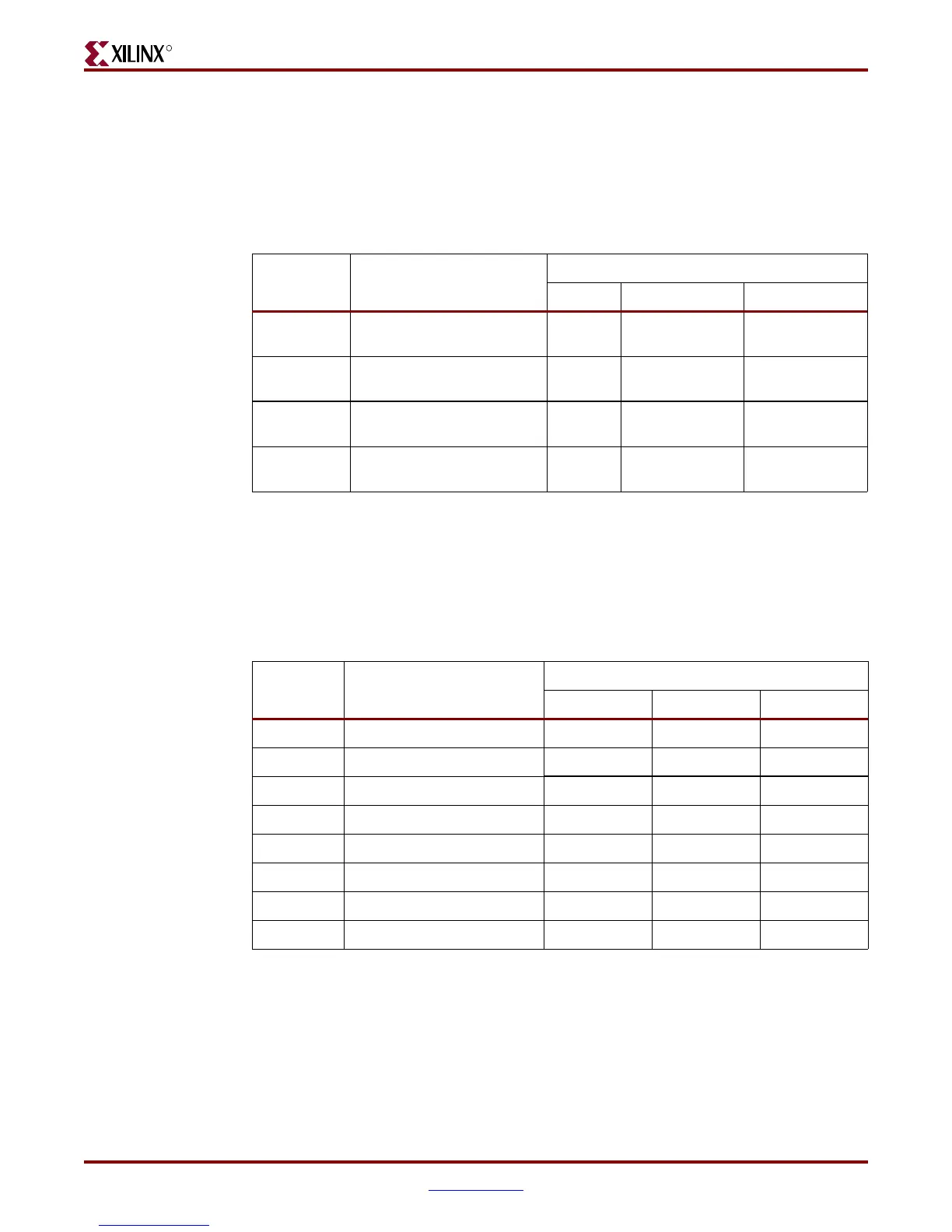
Tabl e 6: Oscillator Socket Clock Pin Connections
Label Clock Name
Pin Number
FF665 FF1136 FF1738
OSC Socket
Top 1
IO_L1P_CC_GC_3 D16 K17 M26
OSC Socket
Top 2
IO_L1N_CC_GC_3 E16 L18 L27
OSC Socket
Bottom 1
IO_L8P_CC_GC_4 AC17 AF18 AL27
OSC Socket
Bottom 2
IO_L8N_CC_GC_4 AB16 AE18 AL26
Tabl e 7: SMA Clock Pin Connections
Label Clock Name
Pin Number
FF665 FF1136 FF1738
P IO_L0P_CC_GC_3 D15 H17 J16
N IO_L0N_CC_GC_3 E15 H18 J15
P IO_L9P_GC_3 F20 H19 K30
N IO_L9N_GC_3 G21 H20 L30
P IO_L9P_CC_GC_4 AB15 AH18 AP16
N IO_L9N_CC_GC_4 AC16 AG17 AP15
P IO_L6P_GC_4 AC18 AG18 AM27
N IO_L6N_GC_4 AB17 AF19 AM26
 Loading...
