Schematic Diagrams
B - 1
B.Schematic Diagrams
Appendix B: Schematic Diagrams
Table B - 1
SCHEMATIC
DIAGRAMS
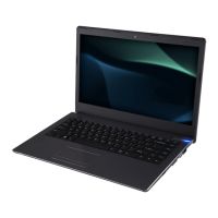
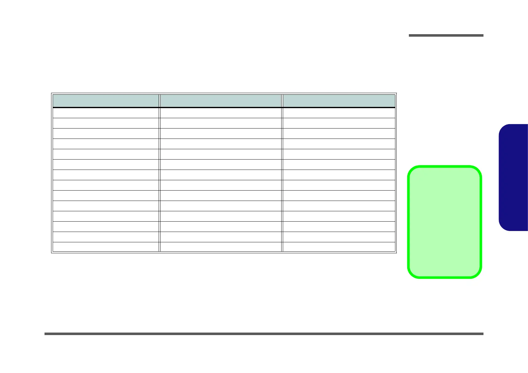
This appendix has circuit diagrams of the N240GU notebook’s PCB’s. The following table indicates where to find the
appropriate schematic diagram.
Diagram - Page Diagram - Page Diagram - Page
System Block Diagram - Page B - 2 Panel - Page B - 16 VCGI, VNN - Page B - 30
Processor 1/9 - Page B - 3 HDMI - Page B - 17 VCore - Page B - 31
Processor 2/9 - Page B - 4 Audio Codec - Page B - 18 1.05VS, 1.8VA - Page B - 32
Processor 3/9 - Page B - 5 SATA, LED, HUB - Page B - 19 AC-In Charger - Page B - 33
Processor 4/9 - Page B - 6 USB Port / TPM - Page B - 20 USB Board - Page B - 34
Processor 5/9 - Page B - 7 Conn, CCD, Fan, Click, TV - Page B - 21 Multi-Board CRT - Page B - 35
Processor 6/9 - Page B - 8 WLAN, 3G/mSATA - Page B - 22 RTL8411B - Page B - 36
Processor 7/9 - Page B - 9 KBC ITE IT8987E - Page B - 23 Pwer SW Board - Page B - 37
Processor 8/9 - Page B - 10 USB - Page B - 24 Click Board - Page B - 38
Processor 9/9 - Page B - 11 Level Shifter 1 - Page B - 25 LED Board - Page B - 39
eMMC - Page B - 12 Level Shifter 2 - Page B - 26 HDD Board - Page B - 40
DDR4 SO-DIMM_0 - Page B - 13 System Power - Page B - 27 Power Sequence - Page B - 41
DDR4 SO-DIMM_1 - Page B - 14 VDD3, VDD5 - Page B - 28
RTD2136N - Page B - 15 1.2V, 0.6VS, 2.5V - Page B - 29
Version Note
The schematic dia-
grams in this chapter
are based upon ver-
sion 6-7P-N24G7-003.
If your mainboard (or
other boards) are a lat-
er version, please
check with the Service
Center for updated di-
agrams (if required).
 Loading...