Service Manual
19
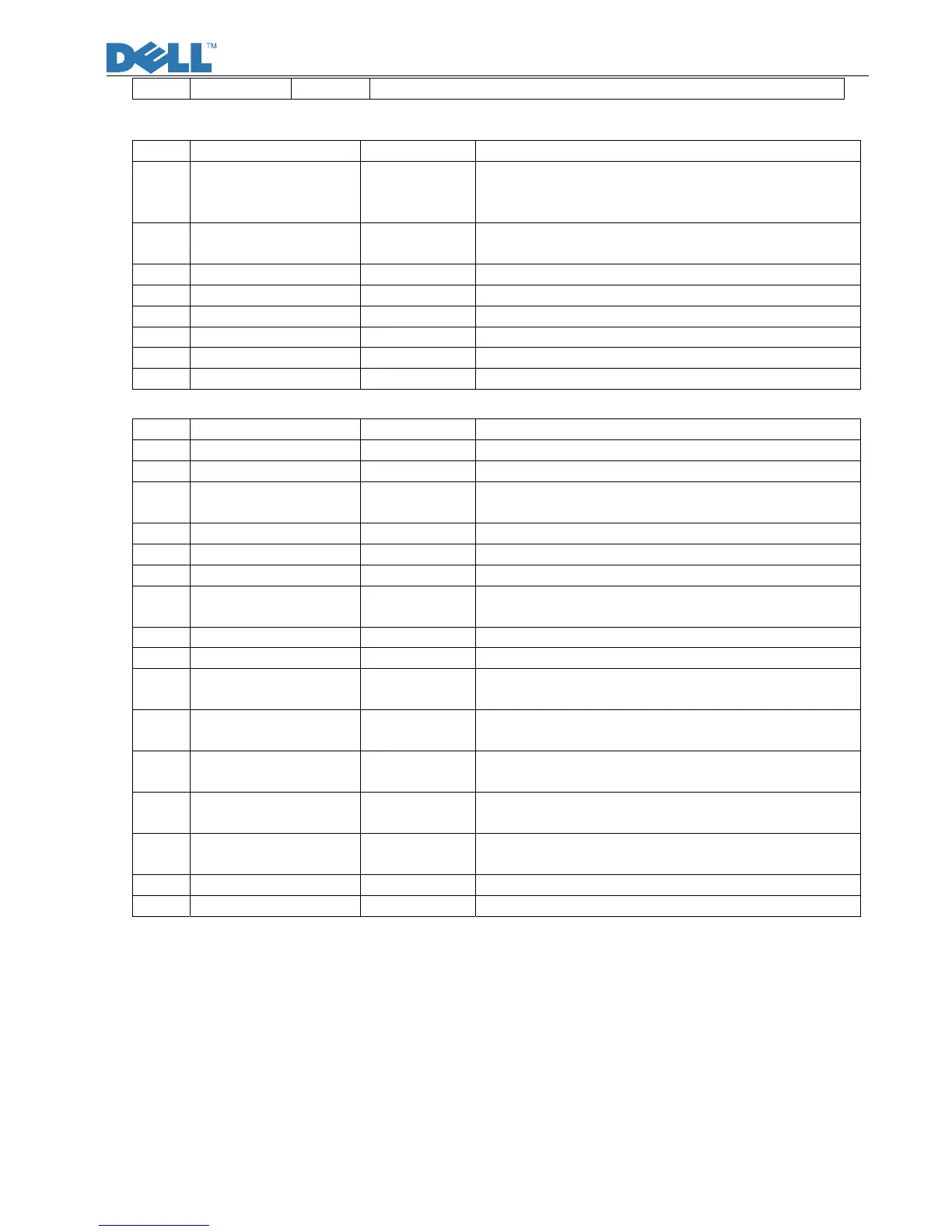
8 VDD P To provide power supply.
8.3 U850 (LD7575, PWM Power Controller)
Pin Symbol I/O Description
1 RT To program the switching frequency. By
connecting a resistor to set the switching
frequency.
2 COMP I Voltage feedback pin. The PWM duty cycle is
controlled by COMP.
3 CS I Current sense for over current protection
4 GND Ground
5 OUT O PWM output
6 VCC I Power supply
7 NC Unconnected
8 HV I To provide the startup current for the controller.
8.4 U1 (INL837, CCFL Inverter controller IC)
Pin Symbol I/O Description
1 DRV1 O Drive output1
2 VDDA I Supply voltage input
3 DIM I Internal LPWM dimming or external PWM pulse
input for dimming function
4 ISEN I Current sense feedback
5 PID I Analog dim input
6 RSTR I Resistor to set striking frequency
7 RT I Resistor to set operating frequency
compensation range
8 ENA I ON/OFF control of IC
9 VSEN I Voltage sense
10 OVPT I Over-voltage/over-current protecting threshold
setting
11 LCT I Timing capacitor to set internal PWM dimming
frequency
12 SSTCMP I Capacitor for soft start time and loop
compensation
13 CT I Timing resistor and capacitor for operation and
striking frequency
14 TIMER I Timing capacitor to set striking time and
shutdown delay time
15 GNDA I Ground
16 DRV2 O Drive output2
 Loading...