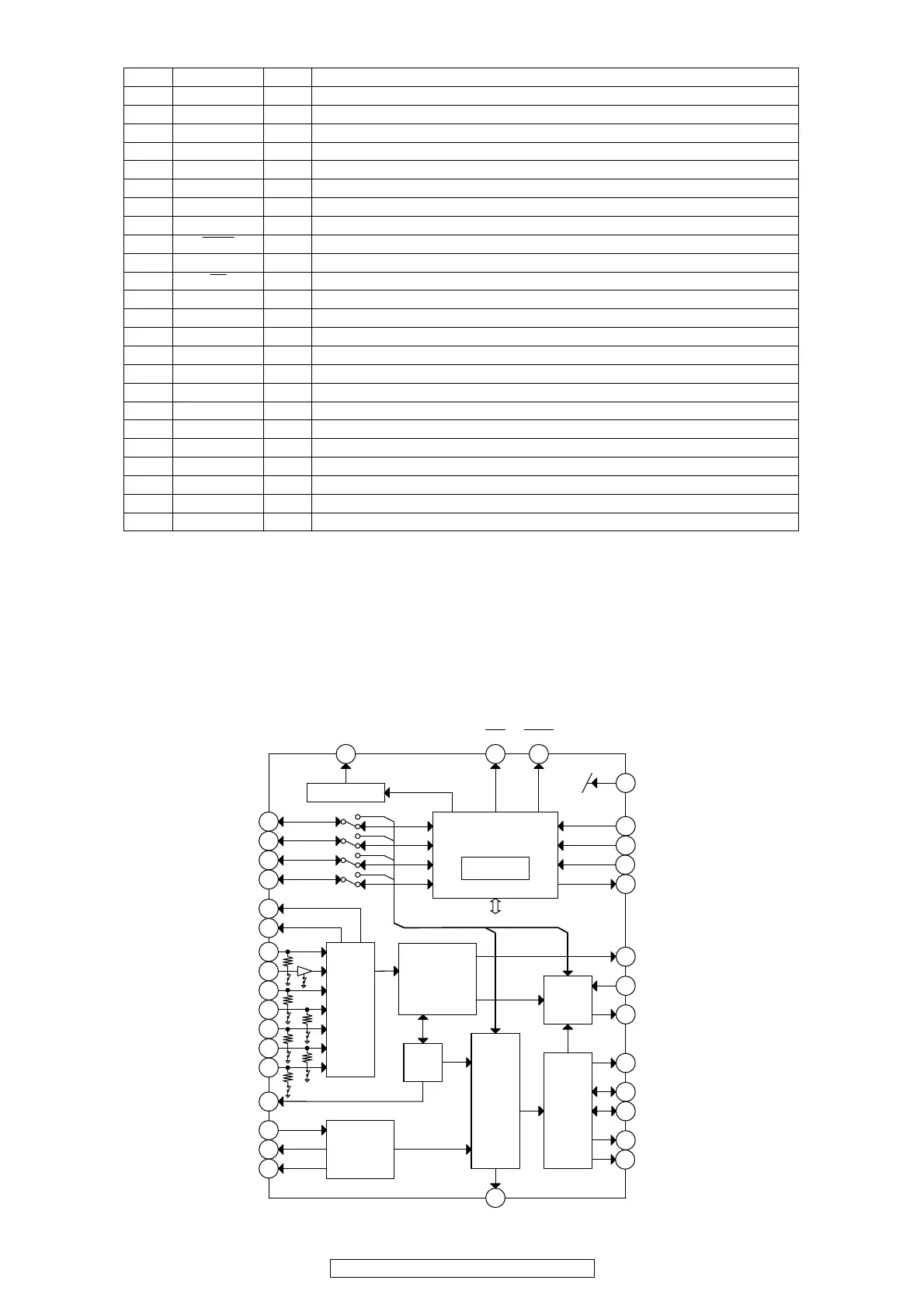
Pin No. Name I/O Function
25 DGND Digital GND
26 DV
DD
Digital power supply (3.3V)
27 XMCK O
Oscillation amplifier clock output pin
28 XOUT O
Output pin connected to the resonator
29 XIN I
External clock input pin, connected to the resonator (12.288MHz/24.576MHz)
30 DV
DD
Digital power supply
31 DGND Digital GND
32 MOUT I/O Emphasis information || Input fs monitor output || Chip address setting input pin
33
AUDIO
I/O
Channel status bit 1 output || Chip address setting input pin
34 CKST I/O
Clock switching transition period signal output || Master/slave setting input pin
35
INT
I/O
Microcontroller interrupt signal output || Pins44-48 I/O setting input pin
36 RERR O PLL lock error, data error flag output pin
37 DO O CCB microcontroller I/F, read data output pin (3-state)
38 DI I
5
CCB microcontroller I/F, write data input pin
39 CE I
5
CCB microcontroller I/F, chip enable input pin
40 CL I
5
CCB microcontroller I/F, clock input pin
41 XMODE I
5
System reset input pin
42 DGND Digital GND
43 DV
DD
Digital power supply (3.3V)
44
GPIO0 O/I General-purpose I/O pin || Selector input pin (output referred to RDATA pin)
45
GPIO1 O/I General-purpose I/O pin || Selector input pin (output referred to RLRCK pin)
46
GPIO2 O/I General-purpose I/O pin || Selector input pin (output referred to RBCK pin)
47
GPIO3 O/I General-purpose I/O pin || Selector input pin (output referred to RMCK pin)
48
RXOUT2 O RX0-6 input S/PDIF through output pin 2
* Input voltage: I= -0.3 to 3.6V, I
5
= -0.3 to 5.5V
* Output voltage: O= -0.3 to 3.6V
* Pins 2, 4, 5, 8, 9, 10, 24, 38, 39, 40, and 41 have an internal pull-down resistor (pd).
Their level is fixed when they are unselected.
* Pins 32 and 33 are input pins for chip address setting when pin 41 is held at the low level.
* Pin 34 serves as the input pin for designating as the master or slave when pin 41 is held at the low level.
* Pin 35 serves as the input pin for configuring the I/O of pins 44 to 47 when pin 41 is held at the low level.
* The DV
DD
and AV
DD
pins must be held at the same level and turned on and off at the same timing to preclude
Latch-up conditions.
 Loading...