19
AVR-2802/982
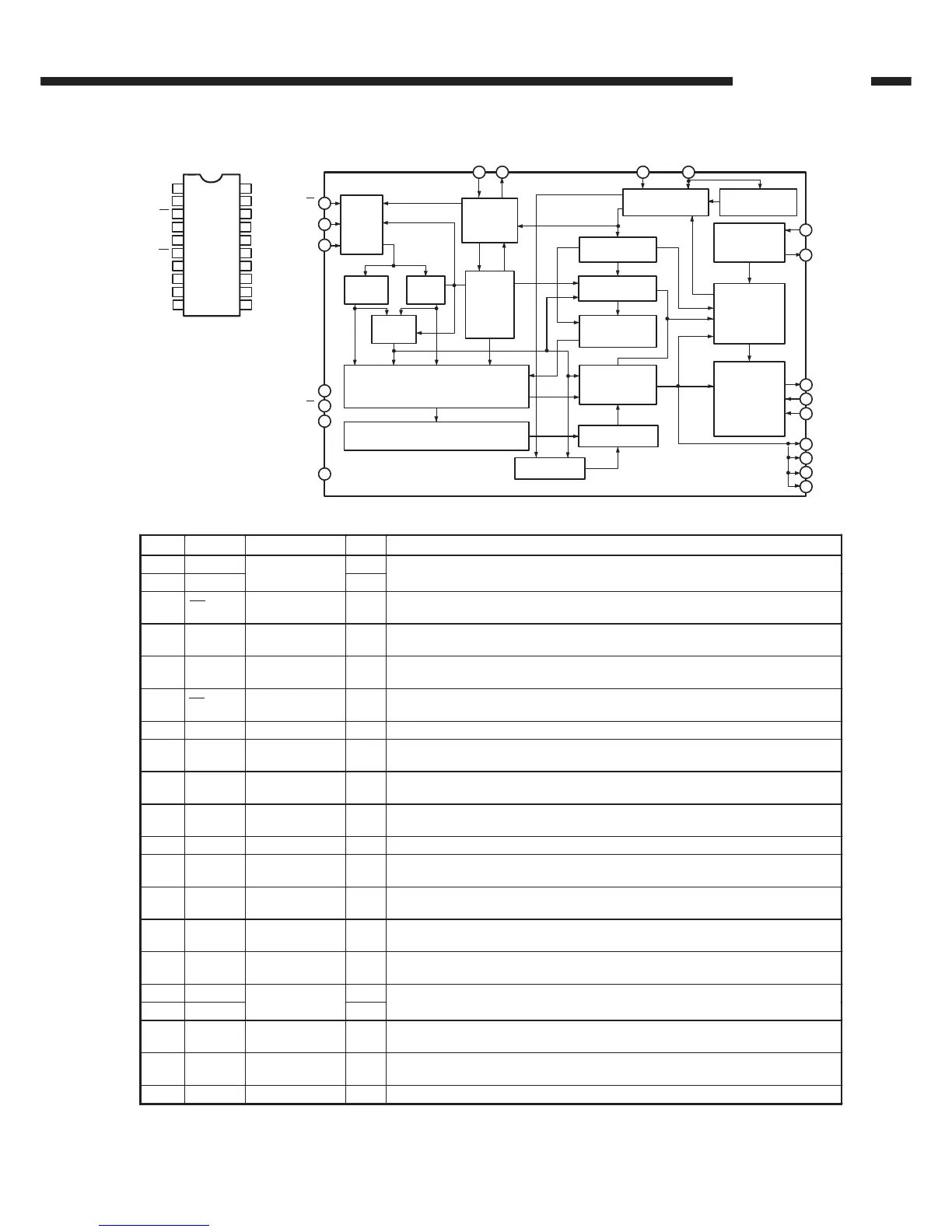
M35015-210SP Terminal Function
Pin No. Symbol Name I/O Function
1 OSC1 Osc. circuit ext. I External terminal for indication oscillator circuit. Standard OSC. freq. is approx. 7MHz.
2 OSC2 terminal. O With this OSC. freq., decides horizontal indicatin and character width.
3 CS Chip select input I
Chip select terminal and turns to “L” when transfer serial data.
Hysteresis input. Pull up resistor is built-in.
4 SCK Serial clock input I
Takes in serial data of SIN at SCK rise when CS terminal is in “L”.
Hysteresis input. Pull up rersist is built-in.
5 SIN Serial data input I
Serial input of register for indication control and data, and address for indication data
memory. Hysteresis input. Pull up rersistor is built-in.
6 AC Auto-clear input I
Resets internal circuit of IC at “L” mode.
Hysteresi input. Pull up resistor is built-in.
7 V
DD2
Power supply
Power supply terminal of analog system. Connect to +5V.
8 CVIDEO
Combined
video output
O
Output terminal of combined video signal. Outputs 2Vp-p combined signal. Character
output, etc. Overlap CVIN signal and outputs at superimpose.
9 LECHA
Character level
input
I
Input terminal deciding character output level in combined video signal. color of character
is white.
10 CVIN
Combined video
input
I
Input terminal of external combined video signal.
Character output etc. overlap this external combined video signal.
11 Vss Ground
Ground terminal. Connect to GND.
12 P0 Output port p0 O
General output or character background signal BL NK1* output is switchable.
Polarity can be selected at ROM mask.
13 P1 Output port P1 O
General output or character background signal CO1* output is switchable.
Polarity can be selected at ROM mask.
14 P2 Output port P2 O
General output or character background signal BLNK2* output is switchable.
Polarity can be selected at ROM mask.
15 P3 Output port P3 O
General output or character background signal CO2* output is switchable.
Polarity can be selected at ROM mask.
16 OSCOUT O Terminal for external use of sync si
nal OSC. circuit. Use the freq.: 14.32MHz at NTSC
17 OSCIN I system, 17.73MHz at PAL. system, 14.30MHz at MPAL system.
18 HOR*
Horizontal sync
signal
I
Inputs horizontal sync signal.
Hysteresis input.
19 VERT*
Vertical sync
signal
Input vertical sync signal. Hysteresis input. Polarity can be selected at ROM mask.
20 V
DD1
Power supply I Power supply terminal of digital system. Connect to +5V.
Ext. terminal
for sync sig.
OSC. Circuit
M35015-210SP (AU: IC453)
1
2
3
4
5
6
7
8
9
1 0
1 1
1 2
1 3
1 4
1 5
1 6
1 7
1 8
1 9
2 0
O S C 1
O S C 2
C S
S C K
S I N
A C
V
D D 2
C V I D E O
L E C H A
C V I N
V
D D 1
V E R T *
H O R *
O S C I N
O S C O U T
P 3
P 2
P 1
P 0
V s s
C S
S C K
S I N
V
D D 1
2 0
A C
V s s
V
D D 2
P 1
P 0
C V I N
L E C H A
C V I D E O
O S C O U T
O S C I N
H O R *V E R T *O S C 2O S C 1
I N P U T
C O N T R O L
C I R C U I T
I N D I C A T I O N
O S C I L L A T O R
D A T A
C O N T R O L
C I R C U I T
A D D R E S S
C O N T R O L
C I R C U I T
T I M I N G
G E N E R A T O R
I N D I C A T I O N
C O N T R O L
R E G I S T E R
I N D I C A T I O N R A M
I N D I C A T I O N C H A R A C T E R R O M
B L I N K I N G C I R C U I T
S H I F T R E G I S T E R
I N D I C A T I O N
C O N T R O L C I R C U I T
R E A D O U T A D D R E S S
C O N T R O L C I R C U I T
I I N D I C A T I O N L O C A T I O N
D E T E C T I O N C I R C U I T
H C O U N T E R
S Y N C S I G N A L
S W I T C H I N G C I R C U I T
S Y N C S I G N A L D I S -
C R I M I N A T I N G C I R C U I T
O S C C I R C U I T
F O R S Y N C S I G N A L
G E N E R A T I O N
T I M I N G
G E N E R A T O R
N T S C
V I D E O O U T P U T
C I R C U I T
6
1 1
5
4
3
7
1 2 1 9 1 8
1 7
1 6
8
9
1 0
1 2
1 3
P 2
1 4
P 3
1 5
 Loading...