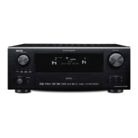
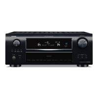
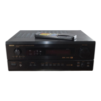
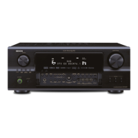
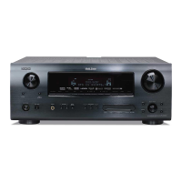
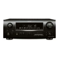
AVR-2802/982
20
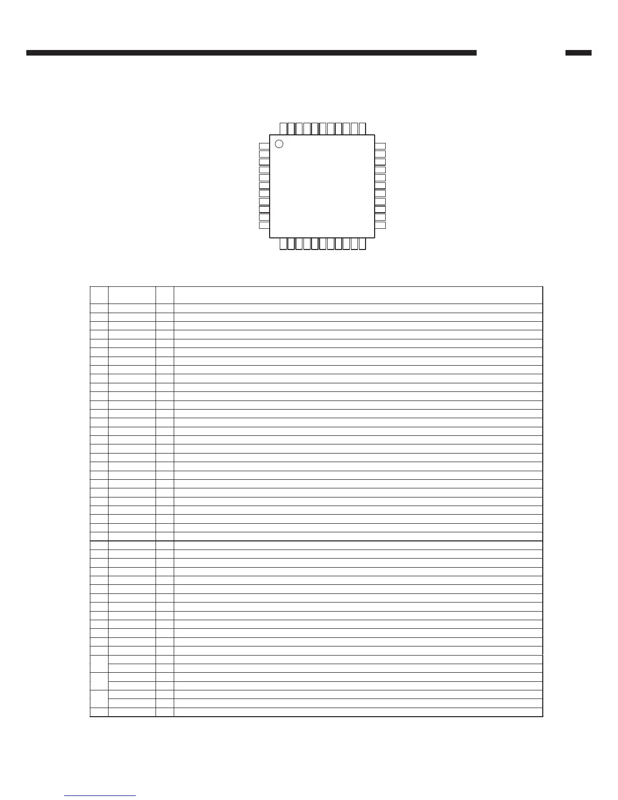
AK4527BVQ (AU:IC602)
AK4527BVQ Terminal Function
1
2
3
4
5
6
7
8
9
10
11
12
13 14
15
16 17 18
19
20
21
22
33
32
31
30
29
28
27
26
25
24
23
44
43
42
41
40
39
38
37
36
35
34
SDOS
I2C
SMUTE
BICK
LRCK
SDTI1
DAUX
DFS
DZF2
RIN+
RIN–
ROUT1
L0OP1
L0OP0/SDA/CDTI
DIF1/SCL/CCLK
DIF0/CSL
P/S
MCLK
DZF1
AVSS
AVDD
VREFH
VCOM
DEM1
TVDD
PDN
ICKS2
CAD1
Top View
LIN+
LIN–
LOUT1
ROUT2
LOUT2
ROUT3
LOUT3
SDTI2
SDTI3
SDTO
DEM0
DVDD
DVSS
ICKS1
ICKS0
CAD0
Pin
No.
Pin Name I/O Function
1 SDOS I SDTO source select pin, L: Internal ADC output, H: DAUX input
2 I2C I Serial control mode select pin, L: 3-core serial, H: I
2
C bus
3 SMUTE I Soft mute pin, H: Soft mute start, L: Release
4 BICK I Audio serial data clock pin
5 LRCK I Input channel clock pin
6 SDTI1 I DAC1 audio serial data input pin
7 SDTI2 I DAC2 audio serial data input pin
8 SDTI3 I DAC3 audio serial data input pin
9 SDTO O Audio serial data output pin
10 DAUX I Auxiliary audio serial data input pin
11 DFS I Double speed sampling mode pin, L: Normal, H: Double
12 NC No Connect, No internal bonding
13 DZFE I Zero input detect enable pin
14 TVDD Power pin for output buffer, 2.7V~5.5V
15 DVDD Digital power pin, 4.5V~5.5V
16 DVss Digital GND pin, 0V
17 PDN I Power down & reset pin, L: Powered-down and register initialized, Reset with PDN when switching CAD0-1
18 TST I Test pin, connected to DVSS
19 NC No Connect, No internal bonding
20 ADIF I Analog Input Format Select pin
21 CAD1 I Chip address-1 pin
22 CAD0 I Chip address-0 pin
23 LOUT3 O DAC3L channel analog out pin
24 ROUT3 O DAC3R channel analog out pin
25 LOUT2 O DAC2L channel analog out pin
26 ROUT2 O DAC2R channel analog out pin
27 LOUT1 O DAC1L channel analog out pin
28 ROUT1 O DAC1R channel analog out pin
29 LIN- I L-ch analog inverted input pin
30 LIN+ I L-ch analog non-inverted input pin
31 RIN- I R-ch analog inverted input pin
32 RIN+ I R-ch analog non-inverted input pin
33 DZF2/OVF O 0 input detect 2 pin/Analog input overflow detect pin
34 VCOM O Common V-out pin, AVDD/2, connect large capacitor to avoid noise
35 VREFH I Ref. V input pin, AVDD
36 AVDD Analog GND pin, 4.5V~5.5V
37 AVss Analog GND pin, 0V
38 DZF1 O 0 input detect pin, H: Input data of G1 is 8192 times “0” in a raw or RSTN bit “0”, L: When P/S= “0”
39 MCLK I Master clock input pin
40 P/S I Parallel/Serial select pin, L: Serial control
DIF0 I Audio data I/F format 0 pin (parallel control)
41
CSN I Chip select pin (3-wire serial control), connect to DVDD when I
2
C bus control
DIFI I Audio data I/F format 1 pin (parallel control)
42
SCL/CCLK I Control data clock pin (serial control), I
2
C=”L”: CCLK (3-wire serial), I
2
C=”H”: SCL (I
2
C bus)
LOOP0 I Loop back mode 0 pin (parallel control), effects digital loop back ADC to all DAC
43
SDA/CDTI I/O Control data input pin (serial control), I
2
C=”L”: CCTI (3-wire serial), I2C=”H” SDA (I
2
C bus)
44 LOOP1 I Loop back mode 1 pin, from SDT1 to all DAC
 Loading...