Block diagram
DQ0
DQ15
UDQM
LDQM
CLK
CKE
CS
RAS
CAS
WE
A10
A0
A9
A11
BS0
BS1
CLOCK
BUFFER
COMMA ND
DEC ODER
ADDRESS
BUFFER
REFRESH
COUNTER
COLUM N
COUNTER
CONTROL
SIGNAL
GENER A TO R
MODE
REGISTER
COLUMN DECODER
SENSE AMPLIFIER
CELL ARRAY
BANK #2
COLUMN DECODER
SENSE AMPLIFIER
CELL ARRAY
BANK #0
COLUMN DECODER
SENSE AMPLIFIER
CELL ARRAY
BANK #3
DATA CONTROL
CIRCUIT
DQ
BUFFER
COLUMN DECODER
SENSE AMPLIFIER
CELL ARRAY
BANK #1
DMn
R
O
W
D
E
C
O
D
E
R
R
O
W
D
E
C
O
D
E
R
R
O
W
D
E
C
O
D
E
R
R
O
W
D
E
C
O
D
E
R
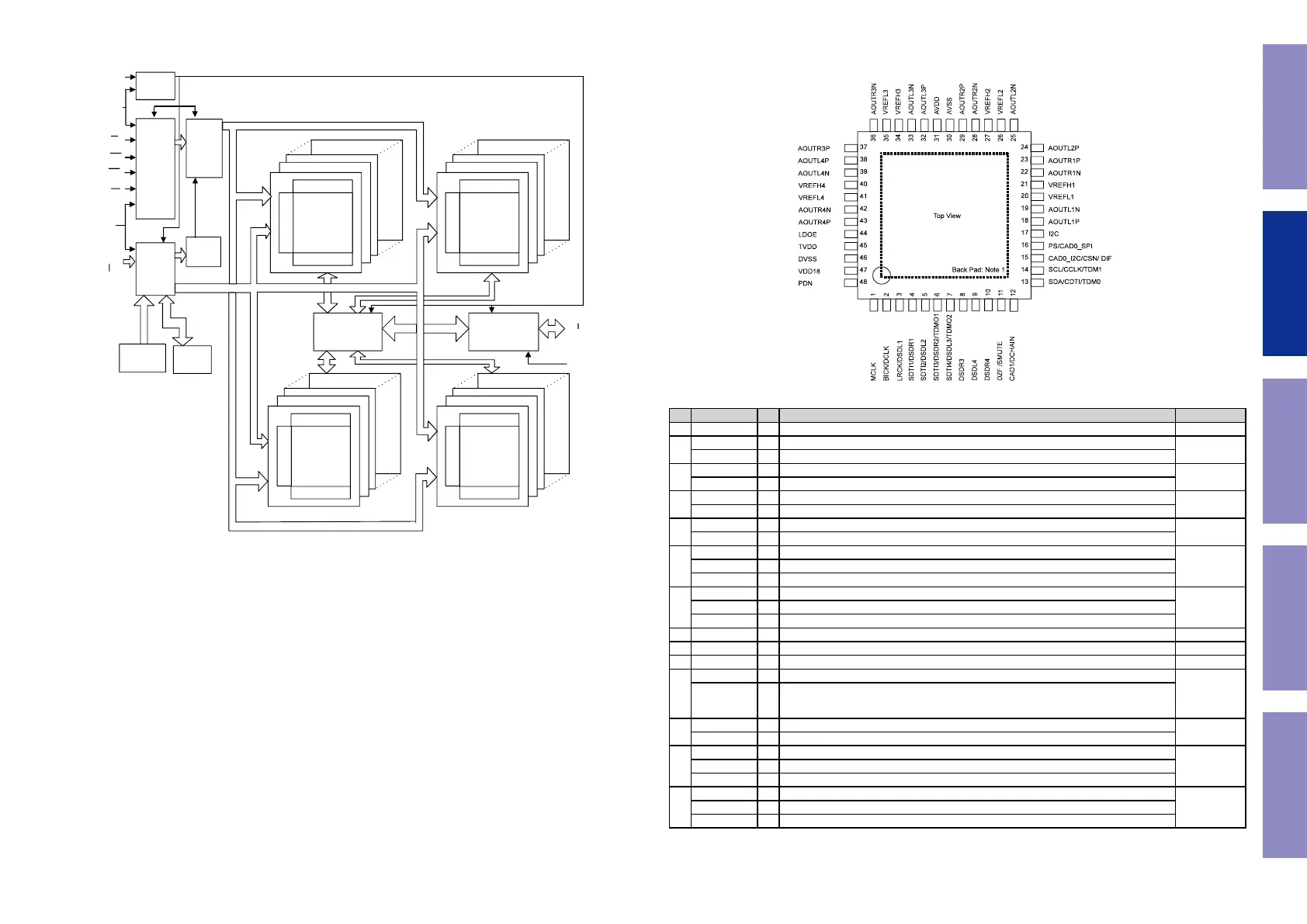
AK4458VN (DIGITAL : U1051)
Pin Function
No. Pin Name I/O Function PD State
1 MCLK I External Master Clock Input Pin Hi-Z
2
BICK I Audio Serial Data Clock Pin in PCM mode
Hi-z
DCLK I DSD Clock Pin in DSD mode
3
LRCK I Input Channel Clock Pin in PCM mode
Hi-Z
DSDL1 I Audio Serial Data Input in DSD mode
4
SDTI1 I Audio Serial Data Input in PCM mode
Hi-Z
DSDR1 I Audio Serial Data Input in DSD mode
5
SDTI2 I Audio Serial Data Input in PCM mode
Hi-Z
DSDL2 I Audio Serial Data Input in DSD mode
6
SDTI3 I Audio Serial Data Input in PCM mode
100k Ω
Pull down
DSDR2 I Audio Serial Data Input in DSD mode
TDMO1 O Audio Serial Data Output in Daisy Chain mode
7
SDTI4 I Audio Serial Data Input in PCM mode
100k Ω
Pull down
DSDL3 I Audio Serial Data Input in DSD mode
TDMO2 O Audio Serial Data Output in Daisy Chain mode
8 DSDR3 I Audio Serial Data Input in DSD mode Hi-Z
9 DSDL4 I Audio Serial Data Input in DSD mode Hi-Z
10 DSDR4 I Audio Serial Data Input in DSD mode Hi-Z
11
DZF O Zero Input Detect in I2C Bus or 3-wire serial control mode
100k Ω
Pull down
SMUTE I
Soft Mute Pin in Parallel control mode.
When this pin is changed to "H", soft mute cycle is initiated. When it is returning to "L", the
output mute is released.
12
CAD1 I Chip Address 0 Pin in I C Bus or 3-wire serial control mode
Hi-Z
DCHAIN I Daisy Chain Mode select pin in Parallel control mode.
13
SDA I/O Control Data Pin in I2C Bus serial control mode
Hi-ZCDTI I Control Data Input Pin in 3-wire serial control mode
TDM0 I TDM Mode select pin in Parallel control mode.
14
SCL I Control Data Clock Pin in I2C Bus serial control mode
Hi-ZCCLK I Control Data Clock Pin in 3-wire serial control mode
TDM1 I TDM Mode select pin in Parallel control mode.
[AK4458]
014011794-E-00 2015/01
- 7 -
5. Pin Configurations and Functions
Ordering Guide
AK4458VN 40
+105 C (Exposed pad is connected to ground)
40 +85 C (Exposed pad is open)
48-pin QFN (0.5mm pitch)
AKD4458 Evaluation Board for AK4458
Pin Configurations
Note 1. The exposed pad at back face of the package must be open or connected to the ground of the board.
Before Servicing
This Unit
Electrical Mechanical Repair Information Updating
57
 Loading...