4-2
4
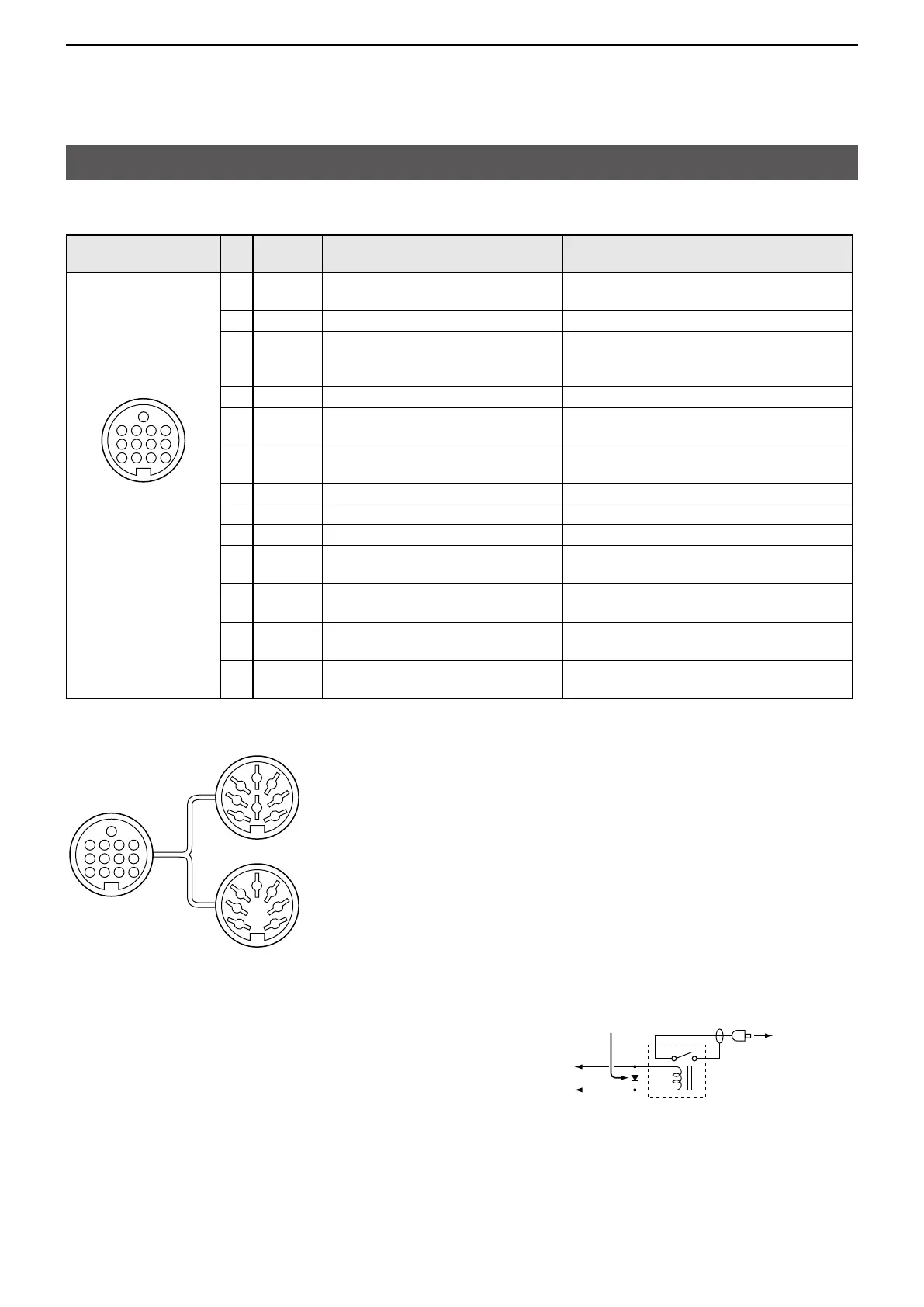
CONNECTOR INFORMATION
[ACC]
Connects to an external equipment or a PC to control an external unit or the transceiver�
ACC
PIN
No.
NAME DESCRIPTION SPECIFICATIONS
1 2 3 4
8765
9
10 11 12
13
Rear panel view
1 8 V Regulated 8 V output�
Output voltage: 8 V ±0�3 V
Output current: Less than 10 mA
2 GND Connects to ground� —
3 SEND
Input/output pin�
Goes to ground when transmitting�
When grounded, transmits�
Ground level: –0�5 V ~ +0�8 V
Input current: Less than 20 mA
4 BDT Data line for the optional AT-180� —
5 BAND
Band voltage output�
(Varies with amateur band)
Output voltage: 0 ~ 8�0 V
6 ALC ALC voltage input�
Control voltage: –4 ~ 0 V
Input impedance: More than 10 kΩ
7 NC — —
8 13�8 V 13�8 V output when power is ON� Output current: Less than 1 A
9 TKEY Key line for the AT-180� —
10 FSKK RTTY keying input�
Ground level: –0�5 ~ 0�8 V
Input current: Less than 10 mA
11 MOD Modulator input�
Input impedance: 10 kΩ
Input level: Approximately 100 mV rms
12 AF
AF detector output�
Fixed, regardless of [AF] position�
Output impedance
: 4.7 kΩ
Output level: 100 ~ 300 mV rms
13 SQL S
Squelch output�
Goes to ground when squelch opens�
SQL open: Less than 0�3 V/5 mA
SQL closed: More than 6.0 V/100 μA
When using the OPC-599 adapter cable
1
1
2
2
3
3
4
4
8
8
7
7
6
6
5
5
9
10 11 12
13
1
2
3
4
76
5
ACC 1
ACC 2
1 FSKK
2 GND
3 SEND
4 MOD
5 AF
6 SQL S
7 13�8 V
8 ALC
1 8 V
2 GND
3 SEND
4 BAND
5 ALC
6 NC
7 13�8 V
When the SEND terminal controls an inductive load, such
as a relay, a counter-electromotive force can malfunction
or damage the transceiver� To prevent this, we recommend
adding a switching diode, such as an 1SS133, on the load
side of the circuit to absorb the counter-electromotive force�
When the diode is added, a delay in relay switching
may occur� Be sure to check its switching action before
operating�
ACC socket
3 SEND
8 13�8 V
Switching diode
Relay
To a non-Icom
linear amplier
(Example) ACC socket
 Loading...