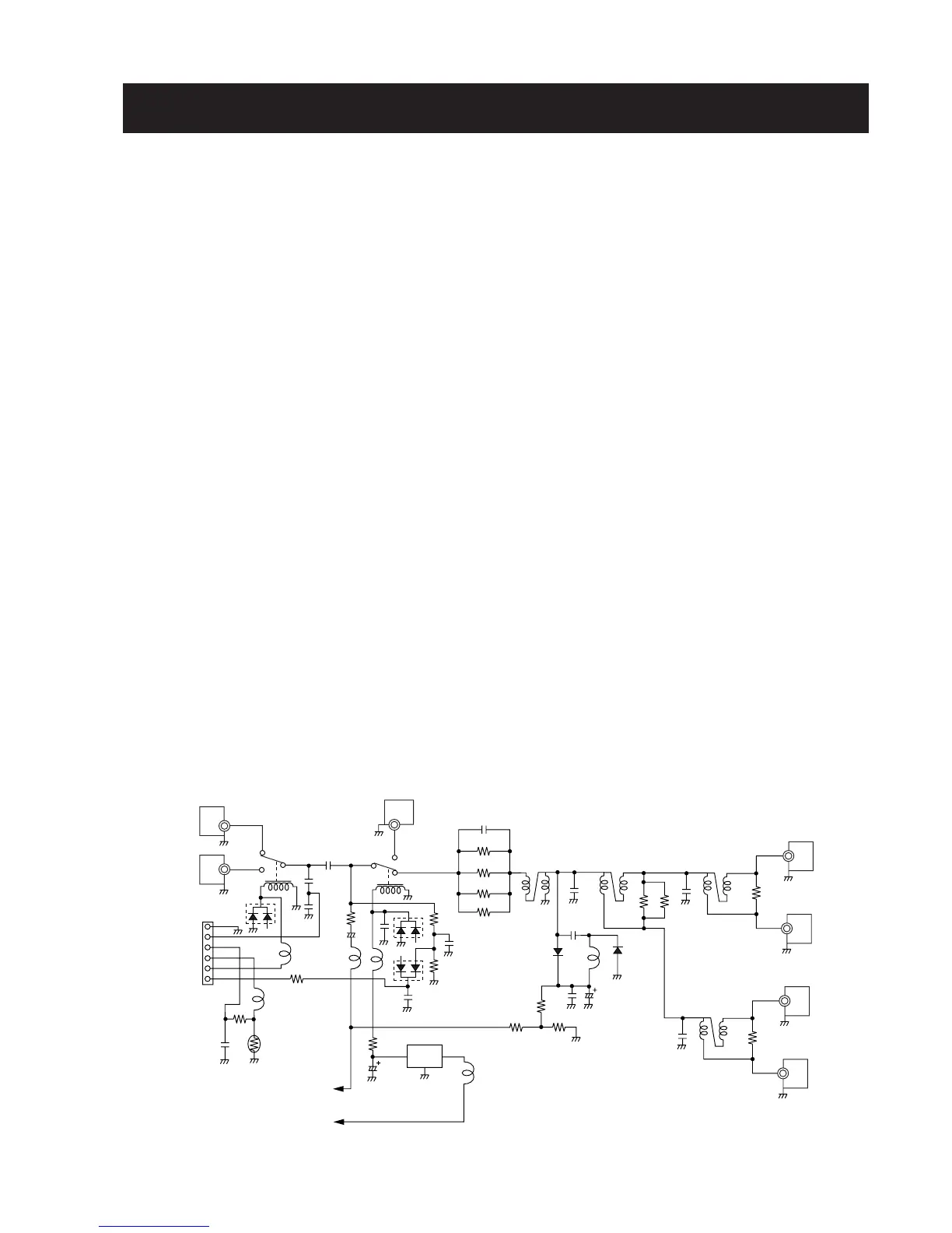
3-1 LINEAR AMPLIFIER CIRCUITS
3-1-1 EXCITER INPUT SWITCHING CIRCUIT
(SPLITR UNIT)
The applied signal from the exciter (transceiver) is passed
through the exciter select circuit (RL1) then applied to the
THROUGH/AMP switching relay (RL2). The switched signal
is passed through the attenuator circuit (R3–R6) when the
amplifier is activated. The attenuated signal is applied to the
power split circuit (L2–L4, L6, R9–R12).
When “THROUGH” is selected, the signal from the exciter
select circuit is applied to the FILTER unit via J8.
The attenuator circuit attenuates the switched signal approx.
1 dB to protect the amplifier circuits from excessive input
power and stabilizes the amplifying operation.
3-1-2 POWER SPLITTER CIRCUIT (SPLITR UNIT)
The power splitter circuit converts the antenna impedance to
1
⁄4 (12.5 Ω) at L2, then the applied RF power level is divid-
ed at the hybrid circuit (L3, R9, R10). The divided RF signals
are separately passed through another hybrid circuit (L4,
R11 and L6, R12) to convert the impedance to 50 Ω and
divide the power level.
The power level divided signal is applied to the one of four
PA units (PA1–PA4) via J4 to J7.
The RF power level at J4, J5, J6 and J7 is approx.
1
⁄5 of
applied power (from the exciter).
3-1-3 POWER AMPLIFIER CIRCUITS
(PA1–4 BOARDS)
The power level divided signal from the SPLITR unit is
amplified at the power amplifier circuit (Q1a/b). The ampli-
fied signal is applied to the COMBINR unit.
Two power MOS-FETs (MRF150) and a negative feedback
circuit are employed for each PA unit to obtain a stable 300
W or higher of RF power and to maintain response gain for
all bands within 3 dB.
3-1-4 POWER COMBINER CIRCUIT
(CONBINR UNIT)
The amplified signals from the PA1 and PA2 boards are
combined at the hybrid circuit (L1, R1) to obtain a 500 W RF
level and the impedance is converted to 25 Ω.
The amplified signals from the PA3 and PA4 boards are
combined at another hybrid circuit (L2, R2).
Both signals are again combined at another hybrid circuit
(L3, R3) to obtain a 1 kW RF level and the impedance is
converted to 12.5 Ω. The combined signal is applied to the
FILTER unit via the impedance convertor (L5) for conversion
to 50 Ω impedance.
3-1-5 FILTER CIRCUIT (FILTER UNIT)
The signal from the CONBINR unit is passed through one of
8 low-pass filters.
The filtered signal is applied to the matching circuit.
SECTION 3 CIRCUIT DESCRIPTION
 Loading...