4 - 2
4-2 TRANSMITTER CIRCUITS
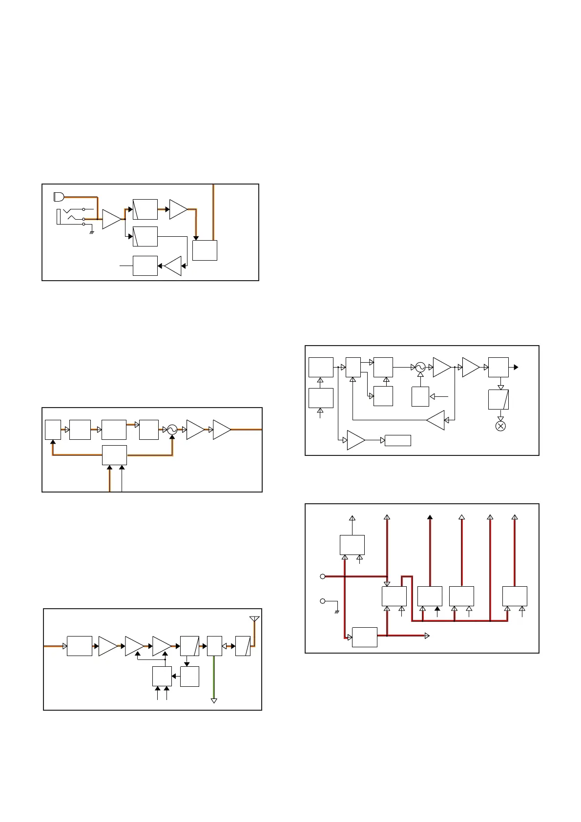
TX AF CIRCUITS
The audio signal from the internal or external microphone
(MIC signal) is applied to the MIC AMP (IC13B). The
amplified MIC signal is passed through the HPF (R266,
C132, C304) and the MIC AMP with pre-emphasis circuitry
(IC3A). The pre-emphasized MIC signal is passed through
the MIC line SW (IC4), and applied to the D/A converter
(IC10).
The level-adjusted MIC signal is applied to the modulation
circuits as the modulation signal.
MODULATION CIRCUITS
The modulation signal from the TX AF circuits are applied to
the VCO to frequency modulate it.
The frequency modulated VCO output is amplified by the
buffer (Q6), amplified by the LO AMP (Q4), then applied to
the TX amplifier circuits via the LO SW (D3 and D4) as the
TX signal.
• TX AF CIRCUITS
HPF
MC1
MIC
AMP
AMP
MIC
AMP
HPF
VOX
[MIC]
OPT
MIC
MIC line
SW
IC4
(PRE-ENPHA)
IC3A
MOD1
VOX DET
D31
IC13A
IC13B
MODIN
• MODULATION CIRCUITS
• TX AMP CIRCUITS
To the TX AMP
BUFF
LO
AMPFILTER
LOOPPLL
IC
D/A
MODIN
CTCSS
Q4Q6
Q76,D59-D61
REF
OSC
X1
IC1
CP
(21.25MHz)
REF.
ADJ.
VCO
DEV
DTC
IC10
TX AMPLIFIER CIRCUITS
The TX signal from the VCO is amplified by the pre-
drive AMP (Q3), drive AMP (Q2) and power AMP (Q1) in
sequence, to obtain the TX output power.
The power-amplified TX signal is fed to the antenna through
the LPFs and antenna SW (D1 and D2).
ANT
LPF
ANT
SW
LO
From
the VCO
SW
PWR
AMP
DRIVE
PRE
APC
CTRL
DRIVE
AMP
LPF
(TX power detector)
To the RX circuits
TXCT3
PWR
DET
D1,D2
D32,D33
IC3B,Q37
Q1
D3,D4
Q3
Q2
• FREQUENCY SYNTHESIZER CIRCUITS
LPF
TX/RX
SW
BUFF
BUFF
LO
AMP
FILTER
LOOP
PLL
IC
BUFF
SHIFT
D3,D4
Q4
Q6
Q5
Q76,D59-61
Ref.freq.
oscillator
X1
IC1
CP
Lock
voltage
OUT
IF DET-IC
IC2
2nd LO
signal
LOOP
Q58
Q13
1st IF mixer
TX AMP
VCO
SHIFT
SW
REF.
ADJ.
VCO
FC
Q77
Q7
4-3
FREQUENCY SYNTHESIZER CIRCUITS
The oscillation frequency of the VCO is determined by the
variable capacitors (D59 and D60). While transmitting, D58
is ON, and C461 and C462 provide the RF path to GND.
This shifts the oscillating frequency range higher. Adding
modulation signal to D61 provides frequency modulation.
The output signal of the VCO is passed through the buffer
AMP (Q6), and applied to the buffer AMP (Q5: for PLL
feedback) or the buffer AMP (Q4: LO AMP).
The output signal of the buffer AMP (Q5: for PLL feedback)
is applied to the PLL IC (IC1). The applied signal is phase-
compared with the reference frequency signal from the
TCXO (X1), and the resulting signal is output from the PLL
IC via the charge pump, and then applied to the VCO as the
lock voltage, after being passed through the loop filter.
Q58 shifts the characteristic of the loop filter for shorter PLL
lockup time when the transceiver needs to lock the PLL up
immediately.
The VCO's power supply circuit (Q11), which works as a
ripple filter, has the capability of fast ON/OFF switching
operation that works even when the transceiver is in the
power save mode.
4-4 VOLTAGE BLOCK DIAGRAM
BATT+
BATT-
T5C
R5C
PSVCO
PCON
CPU5V
AFON
R5
REG
CPU5
REG
IC12,D10
VCC
VCC
SW5
REG
Q55,Q56,
Q78,D39
T5
REG
T5
TX circuits
TX AMP, Backlight
CPU, EEPROM
RX circuits RX/TX circuits VCO
AF power AMP
From the battery
Q22
R5
Q21
REG
VCO5
PS5
Q11
VCO5
Q15,Q16
AF6V
REG
AF
 Loading...