4 - 3
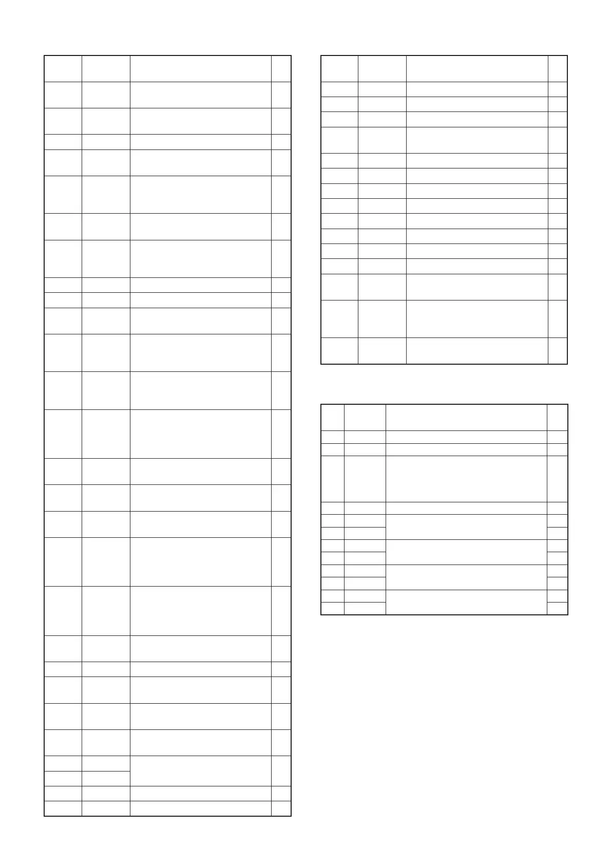
4-5 PORT ALLOCATIONS
• CPU (IC8)
• D/A CONVERTER (IC10)
Pin No.
LINE
NAME
DESCRIPTION I/O
1 MMUT
MIC mute switching.
L=MIC mute.
O
3 TONE
DTMF/1750 Hz tones and beep
sounds.
O
4 CTCOUT CTCSS/DTCS signals. O
10 RESET
CPU reset signal.
H=The CPU is reset.
I
15 CSHIFT
CPU clock shift contol.
H= While the oscillation frequency
is shifted.
O
17 DUSE
DTCS fi lter switching.
H=while the DTCS is in use.
O
18 UNLK
PLL unlock detect.
H= While the PLL circuit is
unlocked.
I
19 NOIS Noise signal. I
22 POWER [POWER] key input. I
23 PTT
External PTT input.
H=An external PTT is pushed.
I
24 SHIFT
VCO oscillation frequency shift
control.
L=While receiving.
O
25 PSVCO
Power supply line for the VCO
switching.
H=While the VCO is activated.
O
26 PS5C
Power supply line "PS5"
switching.
L= While the transceiver is in the
power save mode.
O
27 R5C
Power supply line "R5" switching.
L= While receiving.
O
28 T5C
Power supply line "T5" switching.
L=While transmitting.
O
29 TXC
Transmitting control.
L=TX mute.
O
30 PCON
Power supply line "SW5V"
switching.
H= While transceiver's power is
ON.
O
62 NWC
Discriminator dumping resister
switching.
H= While receiving in the wide
mode.
O
63 INTPTT
Internal PTT input.
L=[PTT] is pushed.
I
64 ITNMIC Internal microphone control. O
65 MIC2
Microphone gain control.
H=MIC gain "L."
O
66 MIC1
Microphone gain control.
H=MIC gain "M."
O
67 LEDC
LCD backlight control.
H=Backlight ON.
O
68 DICK
CONTROL DIAL [VOL] inputs. I
69 DIUD
71–74 KS0–KS3 Keypad scanning signal outputs. O
75–77 KR0–KR3 Keypad inputs. I
Pin No.
LINE
NAME
DESCRIPTION I/O
80 VOX Microphone voice input detect. I
81 VIN Remaining battery voltage. I
83 TEMP The temperature sensing voltage. I
84 SD
RSSI from the IF demodulator IC
(IC2, pin 13).
I
85 CTCIN CTCSS/DTCS signals. I
86 WXALT Weather alert detect. I
87 DASTB D/A converter strobe. O
88 PLLSTB PLL strobe. O
89 DATA Common serial data. O
90 CK Common serial clock. O
94 ESCK Clock to the EEPROM. O
95 ESDA Serial data to/from the EEPROM. I/O
98 SPMUTE
Speaker output control.
H=Speaker mute.
O
99 AFON
AF power AMP control.
L= The AF power AMP is
deactivated.
O
100 RMUT
RX AF line mute switching.
L=AF mute.
O
Pin
No.
LINE
NAME
DESCRIPTION I/O
23 T1 Tuned BPF (D9) tuning voltage. O
24 T2 Tuned BPF (D11) tuning voltage. O
7T3
• While receiving:
BPF tuning voltage.
• While transmitting:
TX power control reference voltage.
O
8 FC Reference frequency adjust voltage. O
10 DET
Squelch threshold level adjustment.
I
11 SQL O
12 DTC
DTCS deviation adjustment.
O
13 MODIN I
18 MODIN
FM deviation adjustment.
I
19 DEV O
20 VOLOUT
Audio output power adjustment.
O
21 VOLIN I
 Loading...