50 Mobile Intel
®
945GM Express Chipset
Development Kit User’s Manual
Hardware Reference
4.6.2.1 478 Pin Grid Array (Micro-FCPGA) Socket
The pin locking mechanism on the CPU socket is released by rotating the screw on the socket 180
degrees counter-clockwise. CPU pins are keyed so as to only allow insertion in one orientation. DO
NOT FORCE CPU into socket. Once the CPU is properly seated into the socket, turn the screw 180
degrees clock-wise to secure the CPU in the socket. Note that the slot on the screw aligns with the
lock and unlock legend on the case of the CPU socket.
Caution: Please refer to the CPU installation instruction in Appendix A prior to inserting the CPU as the
CPU and socket can be easily damaged.
4.6.2.2 PCI Express* (x16)
The platform has one x16 lane PCI Express* Graphics slot and supports either x1 or x16 modes.
The slot is wired “lane reversed” which connects the Intel
®
945GM Express Chipset lanes 0
through 15 to lanes 15 through 0 on the slot. The Intel
®
945GM Express Chipset will internally un-
reverse this wiring since its CFG9 power-on strap is tied low.
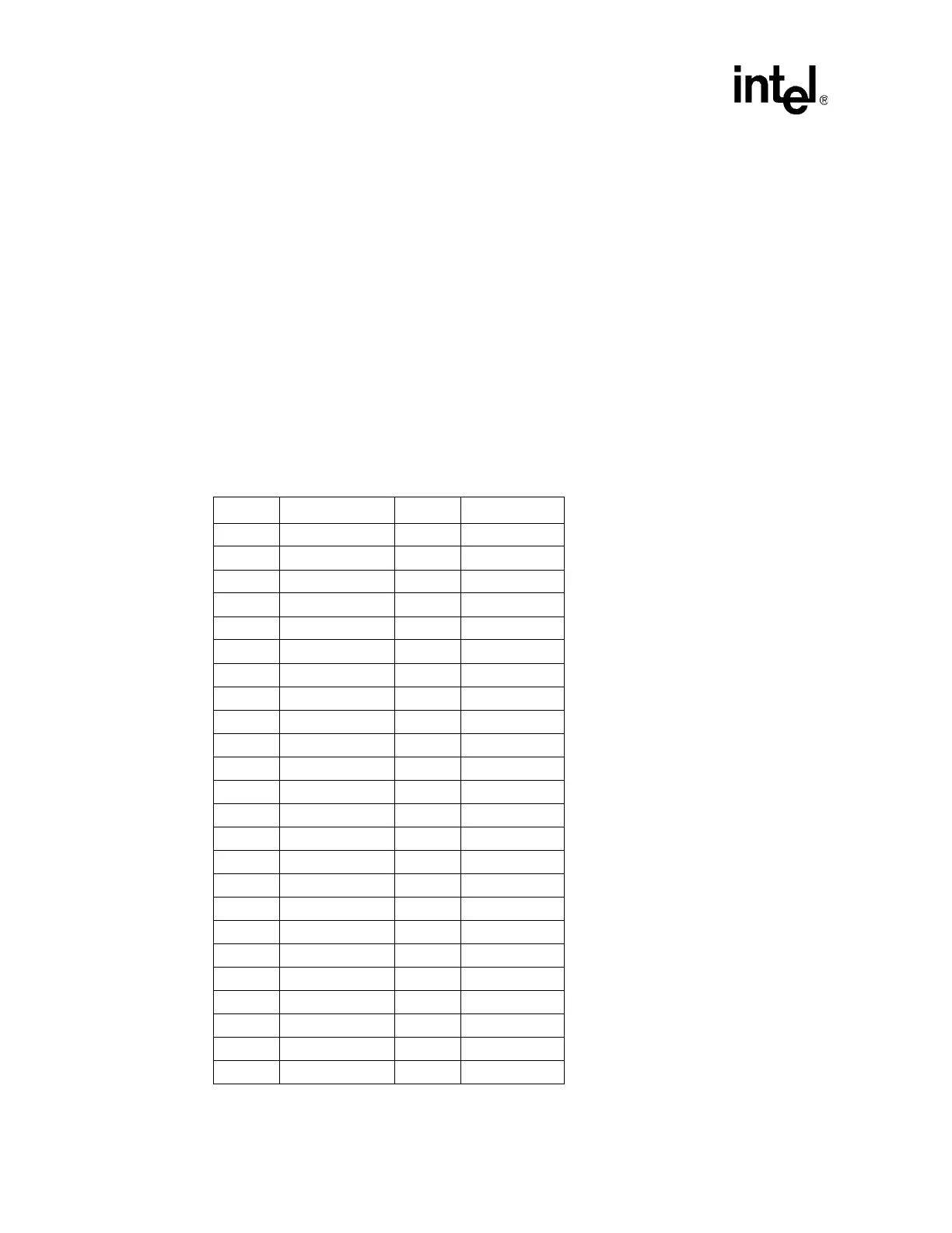
Table 12. PCI Express* (x16) Pinout (J6C1) (Sheet 1 of 3)
Pin Description Pin Description
A1 PRSNT1# B1 +12 V
A2 +12 V B2 +12 V
A3 +12 V B3 +12 V
A4 GND B4 GND
A5 (JTAG) TCK B5 SMCLK
A6 (JTAG) TDI B6 SMDAT
A7 (JTAG) TDO B7 GND
A8 (JTAG) TMS B8 +3.3 V
A9 +3.3 V B9 (JTAG) TRST#
A10 +3.3 V B10 +3.3 VAUX
A11 PERST# B11 WAKE#
A12 GND B12 RSVD
A13 REFCLK+ B13 GND
A14 REFCLK- B14 LANE 0 (T+)
A15 GND B15 LANE 0 (T-)
A16 LANE 0 (R+) B16 GND
A17 LANE 0 (R-) B17 PRSNT2*
A18 GND B18 GND
A19 RSVD B19 LANE 1 (T+)
A20 GND B20 LANE 1 (T-)
A21 LANE 1 (R+) B21 GND
A22 LANE 1 (R-) B22 GND
A23 GND B23 LANE 2 (T+)
A24 GND B24 LANE 2 (T-)
 Loading...


