A THEORY OF OPERATION
4-7
4.5.1.1 Bank Interleaving
Bank interleaving allows the second, third and fourth accesses of a burst read to occur in zero wait
states. The first data access must still pay the entire access penalty. Interleaving significantly improves
memory system performance by overlapping accesses to consecutive addresses. Two-way interleaving
is accomplished by dividing the memory into two 32-bit banks (also referred to as “leaves”):
• one bank for the even word addresses (A2=0)
• one bank for odd word addresses (A2=1)
The two banks are read in parallel and the data from the two banks is multiplexed onto the processor's
data bus. Multiplexing is implemented via the CASxA and CASxB signals. CAS
signals, in addition to
being the Column Address Strobes, are also output enable signals for the DRAM.
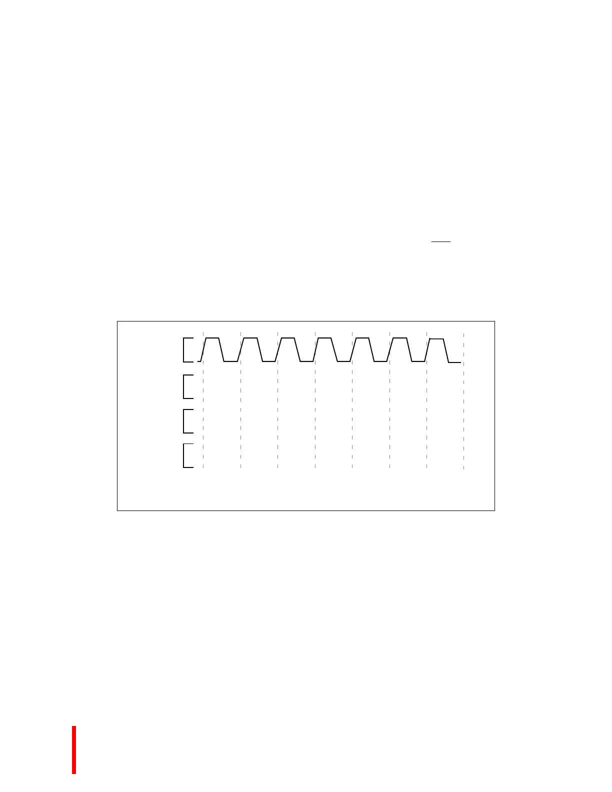
Figure 4-3, Two-way Interleaving, shows DRAM with a 2-1-1-1 quad word burst read wait state profile
being interleaved to generate a 2-0-0-0 wait state system.
Figure 4-3. Two-way Interleaving
4.5.1.2 Wait State Performance
Table 3-4, DRAM Access Times (pg. 3-6) shows the wait state performance for the DRAM; Table 3-5,
DRAM SIMM Configurations (pg. 3-7) shows SIMM module options.
NOTE:
Use 72-pin SIMM modules with 60 or 70ns Fast Page Mode DRAM.
A W
W D
W D
A W
W W
D W
D
A W
W D D D
D
Even Bank
Odd Bank
Processor
CLK
A = Address
W = Wait
D = Data
(Bank A)
(Bank B)
 Loading...


