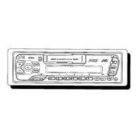
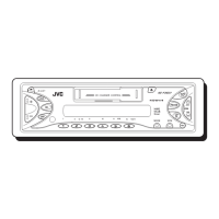
KS-F171
1-16 (No.49774)
SECTION 4
Description of major ICs
4.1 LC75823W (IC651) : LCD driver
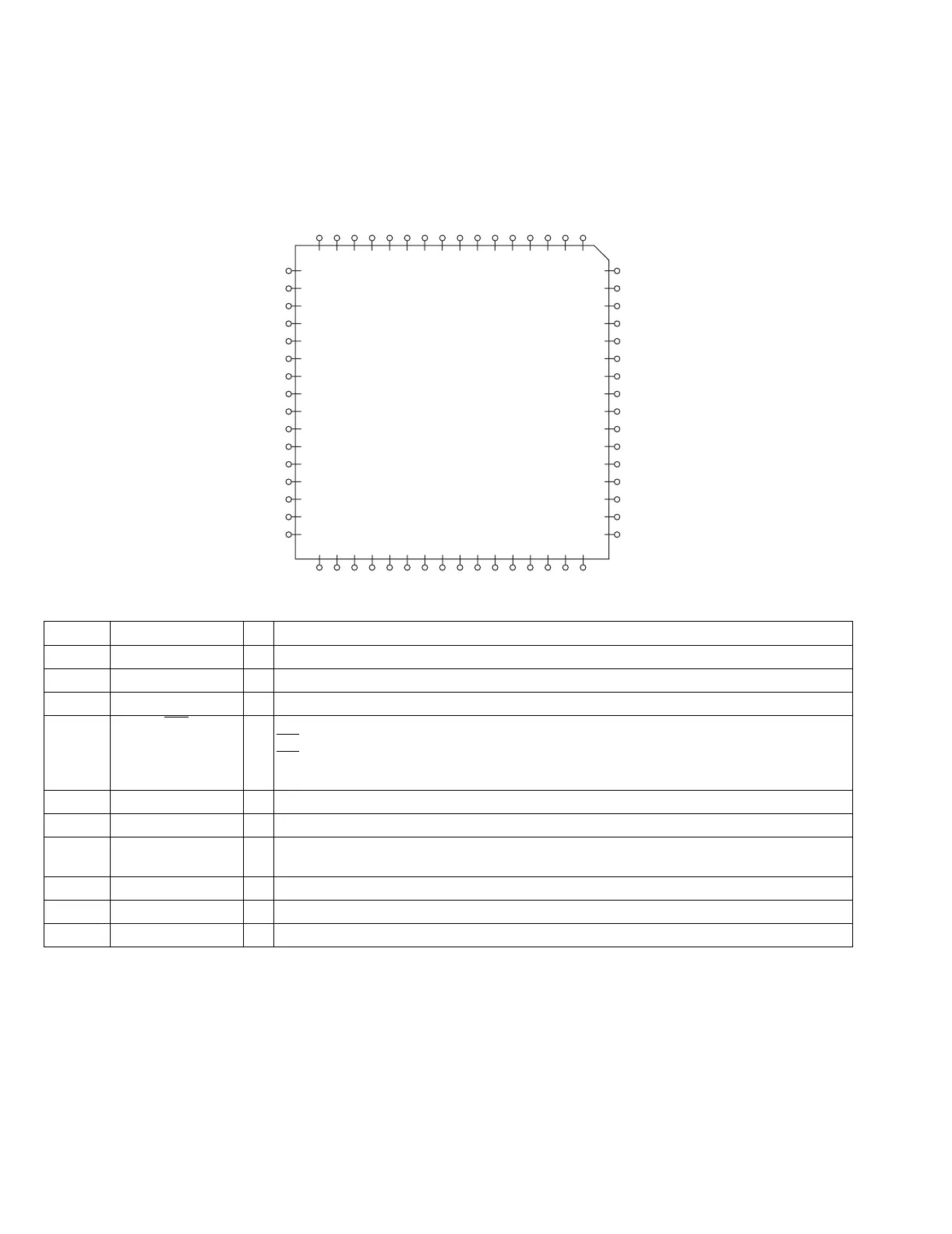
• Pin Layout & Symbol
• Pin function
Pin No. Symbol I/O Functions
1 to 7 -- Non connect
8 to 52 S8 to S52 O Common driver output pins. The frame frequency is given by : t0=(fosc/384)Hz.
53 S53 to S55 -- Power supply connection. Provide a voltage of between 4.5 and 6.0V.
57 INH
I Display turning off input pin.
INT
="L" (Vss) ----- off (S1 to S52, COM1 to COM3="L"
INT="H" (VDD)----- on
Serial data can be transferred in display off mode.
58, 59 Non connect
60 Vss -- Power supply connection. Connect to GND.
61 OSC I/O Oscillator connection.
An oscillator circuit is formed by connecting an external resistor and capacitor at this pin.
62 CE I Serial data interface connection to the controller. CE : Chip enable
63 CLOCK I Serial data interface connection to the controller. CL : Sync clock
64 DATA I Serial data interface connection to the controller. DI : Transfer data
1
2
3
4
5
6
7
8
9
10
11
12
13
14
15
16
S8
S9
S10
S11
S12
S13
S14
S15
S16
17 18 19 20 21 22 23 24 25 26 27 28 29 30 31 32
48
47
46
45
44
43
42
41
40
39
38
37
36
35
34
33
S48
S47
S46
S45
S44
S43
S42
S41
S40
S39
S38
S37
S36
S35
S34
S33
64 63 62 61 60 59 58 57 56 55 54 53 52 51 50 49
S17
S18
S19
S20
S21
S22
S23
S24
S25
S26
S27
S28
S29
S30
S31
S32
DATA
CLOCK
CE
OSC
Vss
INH
VDD
COM3
COM2
COM1
S52
S51
S50
S49
 Loading...