10
- 8
10.1 Scan Time
10.1.2 Time required for each processing included in scan time
10
CPU MODULE PROCESSING TIME
(5) Execution time of various functions processed at END
The execution time of various functions processed at END is the sum of times
required for calendar update, program memory check processing and error clear.
(a) Calendar update processing time
This indicates the time taken to change/read the clock data at END processing
when the clock data set request (SM210 changes from OFF to ON) or the clock
data read request (SM213 turns ON) is issued.
(b) Error clear processing
This indicates the time taken to clear the continuation error stored in SD50 when
SM50 (error clear) rises (changes from OFF to ON).
(c) Program memory check processing time
Note10.5
Note5
This indicates the time taken to make a program memory check when it has been
set in the PLC parameter dialog box of GX Developer.
Time required for program memory check
* 1 : Indicates the step set in the PLC RAS setting (2) of the PLC parameter dialog box. (
Section
8.1.2(5))
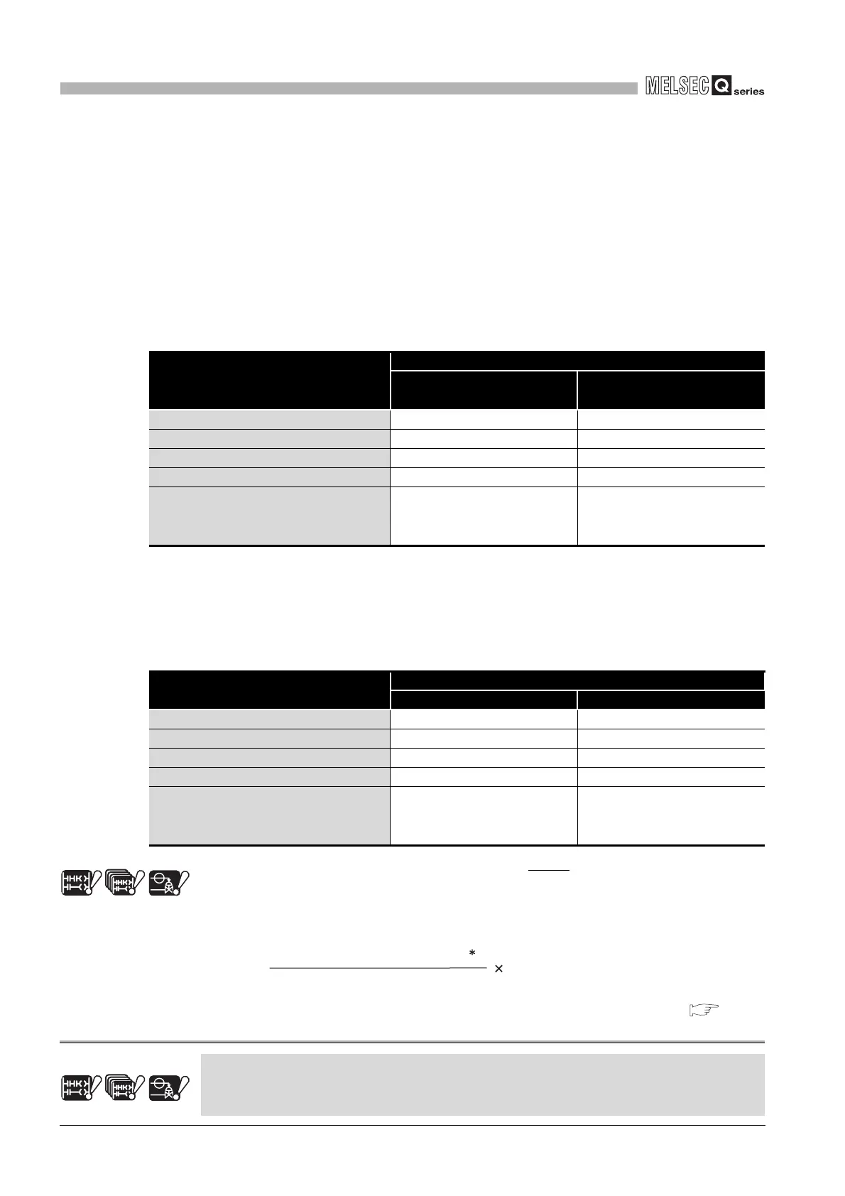
Table10.8 Calendar update processing time
CPU module
END processing time
When clock data set request
is issued
When clock data read request
is issued
Q00JCPU 1.25 ms 0.04 ms
Q00CPU 0.99 ms 0.03 ms
Q01CPU 0.98 ms 0.02 ms
Q02CPU 0.26 ms 0.01 ms
Q02HCPU, Q06HCPU, Q12HCPU,
Q25HCPU, Q12PHCPU, Q25PHCPU,
Q12PRHCPU, Q25PRHCPU
0.11 ms 0.005 ms
Table10.9 Error clear processing time
CPU module
Common processing time
Annunciator Other error
Q00JCPU 2.1 ms 2.0 ms
Q00CPU 1.75 ms 1.7 ms
Q01CPU 1.45 ms 1.35 ms
Q02CPU 1.15 ms 0.41 ms
Q02HCPU, Q06HCPU, Q12HCPU,
Q25HCPU, Q12PHCPU, Q25PHCPU,
Q12PRHCPU, Q25PRHCPU
0.84 ms 0.21 ms
Note5
Basic
High
Performance
Note10.5
Note10.5Note10.5
Process
Since the Basic model QCPU, High Performance model QCPU and Process CPU do not support
the setting for program memory check, it is not necessary to be conscious of this processing
time.
Basic
Note10.5
High
Performance
Note10.5Note10.5
Process
= 3.1 ms
Check capacity per scan (step)
1024
1

 Loading...