6E-4 Transmitter
3.0 Transmitter
3.1 General
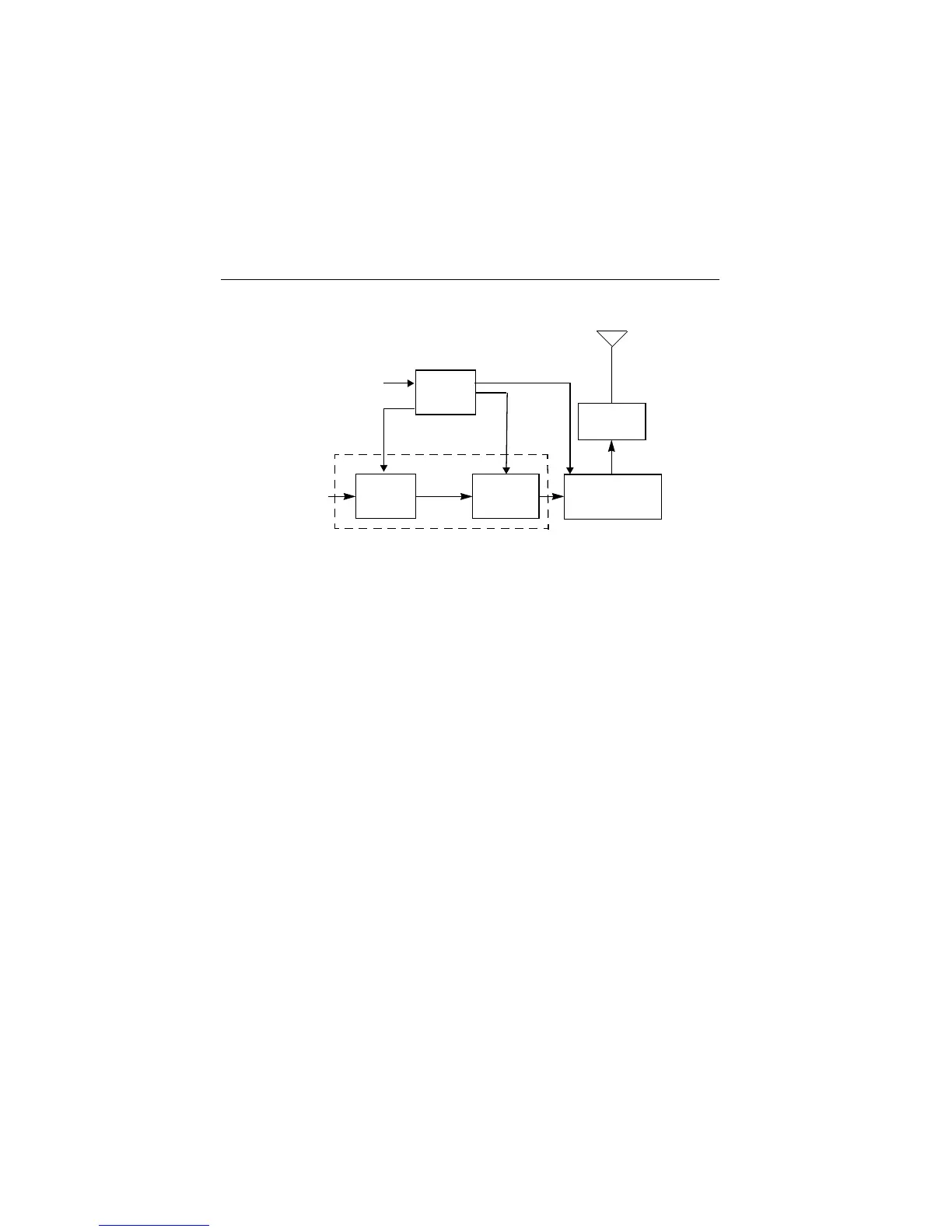
(Refer to Figure 6-1)
The Lowband transmitter consists of the following basic circuits:
1. power amplifier (PA)
2. antenna switch
3. harmonic filter
4. antenna matching network
5. power control integrated circuit (PCIC).
3.1.1 Power Amplifier
The power amplifier consists of two LDMOS devices:
1. PA driver, U101 and
2. PA final stage, Q100.
The LDMOS driver (U101) provides 2-stage amplification using a supply voltage of 7.3V. The
amplifier is capable of supplying an output power of 0.3W (pins 6 and 7) with an input signal of 2mW
at (pin16). The current drain is typically 120mA while operating in the frequency range of 29.7 - 50
MHz. The power output of this stage is varied by the power control loop which controls the voltage on
pin 1.
The LDMOS PA is capable of supplying an output power of 8W with an input signal of 0.3W. The
current drain is typically 2000 mA while operating in the frequency range of 29.7 - 50 MHz. The final
stage gate is bias by a voltage from PCIC pin 24. This voltage is the output of a programmable DAC
inside the PCIC and the output is adjustable with the radio tuner.
Figure 6-1: Lowband Transmitter Block Diagram
PCIC
PA
PA Fin al Antenna Switch/
Driver
Stage
Harmonic Filter
Vcontrol
Gate bias
From
Antenna
Matching
Network
PowerAmplifier (PA)
VCO
Antenna switch bias
SPI bus
 Loading...